|
|
Volume 4 No.2, Spring 2001 |
ISSN# 1523-9926 |
|
|
Volume 4 No.2, Spring 2001 |
ISSN# 1523-9926 |
Antonis K. Koukos
koukosan@otenet.gr
Technological Educational Institution of Chalkis
Electrical Engineering Department
Psahna, 344 00 Greece
ABSTRACT
This paper presents a Header Error Control (HEC) circuit for use in Asynchronous Transfer Mode (ATM) Transceivers. Transceivers, are used in ATM Terminal Adapters (TA) and offer cell (ATM packet of 53 bytes) transmission/reception functions, providing services in upward/downward data directions. Header Error Control, which is a significant function of an ATM Transceiver, consists of error syndrome generation and error detection and correction. The paper introduces the model, the algorithm, and the implemented circuit. The circuit has been implemented on Applications Specific Integrated Circuit (ASIC) chips and can be useful to everyone who develops basic parts of ATM Networks.
INTRODUCTION
The model, the algorithm and the implemented circuit of a Header Error Control (HEC) circuit for use in Asynchronous Transfer Mode (ATM) Transceivers is presented in this paper. Transceivers are mainly used for accessing the ATM Network and offer cell (ATM packet of 53 bytes) transmission/reception functions providing services in upward/downward data directions [1], [2], [3], [4]. Transceivers are used in ATM Terminal Adapters (TA). Header error control is a significant function of an ATM Transceiver, and consists of error syndrome generation and error detection and correction. The other functions are: cell buffering, cell disassembly/assembly and classification, rate decoupling/coupling, information insertion/extraction, connection identity fields extraction and identification, and idle cell discarding functions. The circuit has been implemented on Applications Specific Integrated Circuit (ASIC) chips.
In [5] an ATM layer chip for broadband integrated services digital network applications is described. The chip performs common asynchronous transfer mode layer functions such as cell assembly and disassembly. In cell assembly working mode it uses an external First-in-First-Out (FIFO) memory to temporarily store the cells. It uses a Cyclic Redundancy Check (CRC) code to control the emitted headers for errors. In cell disassembling working mode it offers CRC capabilities to detect and correct the cell headers errors. In addition it stores the received cells in an external FIFO memory. It must be noted that the ATM layer chip was the first experimental implementation offering terminal adaptation functions for ATM Networks.
In [6] an efficient parallel adapter for computer interface to the ATM Network is described. An ATM parallel adapter is realised as a single chip two-dimensional array (XILINX’s family). The component operations include cell header recognition and acceptance (connection identity recognition), header error control syndrome generation, and header error detection. Unfortunately, the circuit does not offer header error correction. In addition, the circuit can only support four active connections simultaneously.
In a new transceiver [7], [8], which solves all these problems, header error control functions are supported. In particular, header error control syndrome generation is supported at the transmission side as well as header error detection and correction functions which are supported at the reception side. The transceiver circuit, which has flexibility for use in PC terminals or in inter-working units and switches, implements functions of the lower layers of the ATM Protocol Reference Model (PRM). This type of transceiver circuit can be very useful to everyone who develops basic parts of ATM Networks.
THE MODEL
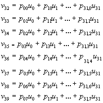
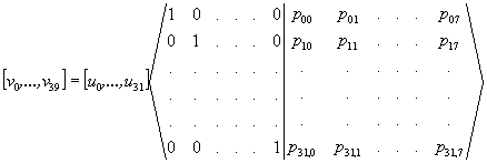
The transceiver manipulates cells with 53-byte headers. We use a CRC scheme to control for the errors. Every header consists of m (m = 32) used (or message) bits (m0, m1,…, m31) followed by r (r = 8) check bits (r0, r1,…, r7), and the total number of bits n = m + r (n = 40) bits (n0, n1,…, n39). Such a code consists of code-words v = (v0, v1,…,v39) which are produced from the 32-bit sequence u = (u0, u1,…, u31) with linear combinations of it. The 8 check bits (r = n – m =40-32=8) are the last bits of the codeword v and produced by the 32 bits according to rules with the form [9]
 (1)
(1)
The above pij coefficients have the value 0 or 1 and participate in modulo-2 calculations. We can rewrite the equation (1) as
 (2)
(2)
or ![]() (3)
(3)
where G is the generator matrix and determines the (40, 32) linear block code.
G matrix has the form
![]() (4)
(4)
where I32 is the identity matrix of class 32.
In our case we use cyclic code (a code where a codeword cyclic shifting gives a valid codeword) where a codeword is expressed by a polynom as
![]() (5)
(5)
Such a polynom is a valid codeword if and only if
![]() (6)
(6)
So that, the transmitted headers consist of codewords, which are multiple of a polynom g(X). In the reception side, the received headers should be multiple of g(X) in order to be non-erroneous codewords.
THE ALGORITHM & THE CIRCUIT
Before cells emitted (Transmitter side), header error control is realised according to a CRC method as recommended by [4] (Fig. 1), which based on the equations (7):
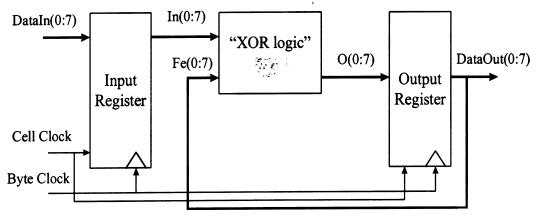
Figure 1. Header Error Control circuit (Transmitter side)
 (7)
(7)
The circuit is fed by the first four header bytes sequentially (In(0:7)) according to cell and byte clocks timing [4], [7], [9]. According to this, the produced data (DataOut(0:7)) are supplied as feedback to the system (Fe(0:7)), thus implementing the production of the fifth header byte (error control byte), which is used for controlling the header errors. This method uses the characteristic polynom g(X)=X 8+X 2+X+1. For reducing the probability of loosing synchronisation by the receiver (due to shifting), a specific byte (coset) is added after the error control byte.
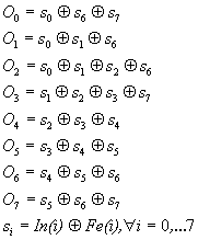
In the receiver side, the error detection and correction is based on Hamming distance (the number of different bit positions between two codewords) [9]. The code examines if the received bits sequence is a valid codeword or not (error detection). If it is invalid, then it tries to correct the error(s) by using the Hamming distance.In our case a parallel scheme (on a byte basis) is used to perform the cyclic redundancy code check (header error detection operation). This is performed by decoding the syndrome that was coded by the symmetrical operation of a transmitter. A polynomial division of this bit-stream by the characteristic polynom X8+X2+X+1 is done. If the remainder of the division equals to zero, this means that the header is not erroneous (NO_Errors = 1). It uses a ‘xor’ logic circuit similar to that in Figure 1 based on a specific set of equations [4]. The circuit is fed by the five header bytes [8]. The circuit produces an 8-bit output O(0:7) which depends on 8 input bits In(0:7) (every received header byte) and on 8 feedback bits q(0:7) from the circuit output O(0:7). The implemented circuit equations are
 (8)
(8)
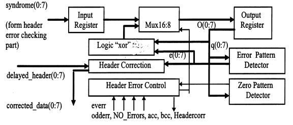
Figure 2. Header error correction circuit (Receiver side)
It is possible there are single or multiple errors. Single error means that only one bit of the header transferred data has been changed. Multiple errors means that two or more bits of the header transferred data have been changed. There are odd class errors (1,3,5,…), (Odderror = 1), and even class errors (2,4,6,…), (Everror = 1).
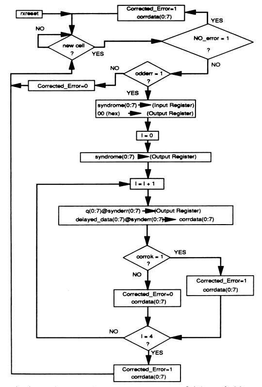
Figure 3. Header Error Correction Algorithm (Receiver Side)
The correction operation uses a ‘xor logic’ circuit implemented by the same set of equations (7), where Oi is the output bit, qi the input bit (the output of the header error detection for the first byte of the header (syndrome(0:7)) and then the previous Oi output) and ei the bit from an error pattern detector with Si = qi Å ei).If there are odd-class error(s) then the syndrome(0:7) (from header error detecting part) is loaded to the input register. Then input register contents are transferred to output register contents (I=0). In the next step (I=I+1, according to a byte clock) the combination of q(0:7) with the e(0:7) (synderr(0:7)) is loaded to the “xor logic” circuit and its output is loaded to the output register. Simultaneously, the delayed received header data (delayed_data(0:7)) are combined with e(0:7) (synderr(0:7)) data in the header correction part. Its last part output is the corrected_data(0:7). If error correction has been done (corrok =1) then the circuit provides to its output the corrected data and activates the Corrected_Error signal (Figure 3). Then, the system halts until the arrival of the next ATM cell.
The Error Pattern Detector gives the value ‘one’ to the position that corresponds with the erroneous bit in every byte of the header, as the following patterns describe: 10000000, 01000000, 00100000, 00010000, 00001000, 00000100, 00000010, 00000001 (e(0:7)). If the header is corrected a zero pattern detector output is activated (Headercorr=1), (Figure 2). The scheme corrects only single bit errors, detects double bit errors and some of higher-class bit errors.
SUPPLEMENTARY FUNCTIONS
HEC error detection and correction can be designed with cell delineation function (Figure 4). This function is responsible for recovering ATM cell limits. Cell delineation can be implemented easily using a three-phase algorithm. During the first phase (HUNT) the receiver chooses an incoming random 40-bit (or 5 bytes) sequence and calculates its syndrome. If it has a zero value, then a particular cell header has been found and the receiver knows the cell limits. Otherwise, a 1-bit shift occurs and the receiver searches for a new correct header.
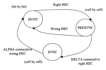
Figure 4. ATM Cell Delineation
In the next phase (PRESYNC) the system checks for the correctness of successive cells by counting the correct header number. If this number (DELTA: a positive number greater than 1) has a particular value, then the system operation will be transferred to the last phase (SYNC). Otherwise, it returns to the first phase. During this last phase (where synchronisation has been succeeded) it continues header error checking. If a number (ALPHA: a positive number greater than 1) of successive cell headers are erroneous (lost of synchronisation), then the system operation will be transferred to the first phase, and a header error counter will be reset.
RESULTS & CONCLUSIONS
In this paper a header error control circuit for ATM transceivers is presented. Header error control, which is significant function of an ATM transceiver, consists of error syndrome generation, error detection & correction. The circuit has been implemented on Applications Specific Integrated Circuit (ASIC) chip. The paper content-flow has as follows: in the beginning a general introduction of the circuit is done. In the following the model of the circuit functionality is discussed in detail. The operation algorithm and the circuit implementation are discussed by using suitable block diagrams and flow charts. The following two figures show the results of the circuit implementation.
Figure 5 shows a snapshot of the header error syndrome generation in the transmitter side. The first 8 signals (INDOUT(0:7)) are inputs to the error syndrome generation circuit. The TXHECDATA(O:7) are the outputs of this cicruit. Finally, the TXHECDIS signal enables or disables the error control circuit operation [7].
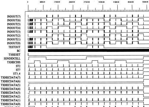
| Figure 5. Results of Transmitter: Header error control syndrome generation: INDOUT(0:7)) : inputs to the error control syndrome generation circuit, TXHECDATA(O:7) : outputs of this cicruit, TXHECDIS : enables or disables the error control operation. |
Figure 6 shows a snapshot of the ATM network interface (IF) where, ATMDIN is the input of cell data and RXDATA(0:7) is the output of the receiver. HEADOK and HEADCR signals are activated to show that the cell header has no errors and the correction operation has been completed [8].
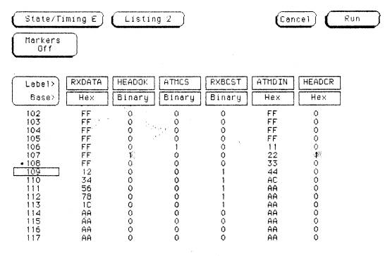
| Figure 6. Experimental Results of Receiver: Header Error Correction: ATMCS: ATM Network cell start signal, ATMDIN(0:7): ATM Network received data signals, RXDATA(0:7): Rec. output data signals, HEADOK: Non-erroneous header signal, HEADCR: Corrected Header signal, RXBCST: Rec.buffer cell start signal. |
Kawarasaki, M. and Jabbari, B.,
“B-ISDN Architecture and Protocol,” IEEE Journal on Selected Areas
in Communications, Vol. 9, No 9, pp. 1405-1415, Dec. 1991.
De Prycker, 1993, Asynchronous
Transfer Mode, Solution for Broadband ISDN.
Horwood.
Black Uyless: “ATM Foundation for
Broadband Networks,” Volume 1, Prentice
Hall, Second Edition, 1999.
CCITT, “B-ISDN User Network
Interface,” Draft Rec. I. 432.
Johnston, A., and Chao, A., J., “The
ATM Layer Chip An ASIC for B-ISDN
Applications,” IEEE Journal on Selected Areas in
Communications, Vol. 9, pp.741-750, 1991.
Koukos, A.K., Doumenis, G.A.,
Papadopoulos, A.I., and Reisis, D.I., “An
efficient Parallel Adaptor for Computer Interface to the
ATM Network,” IMACS-P.D.COM '91,
Corfu, pp. 435-439, 1991.
Koukos, A.K., Kamaras, J.G., and
Protonotarios, E.N., “An Efficient Transmitter Chip for ATM Networks,”
TELECOM’97, Varna, Boulgaria, pp. 39-45, 1997.
Koukos, A.K., Kamaras, J.G., Catsoulis,
A.C., and Protonotarios, E.N., “An
Efficient Receiver Chip for ATM Networks,”
International Conference Electronic Circuits & Systems ‘97,
Bratislava, pp. 231-234, 1997.
LIN, S., and COSTELLO, D.J., “Error Control Coding,” Prentice Hall, 1993.
Return to This Issues Home Page