) which is a "NOT" function.
the Technology Interface / Spring98
Real numbering systems are characterized by the fact that they
can be manipulated by the four basic arithmetic operations of
addition, subtraction, multiplication, and division. Coded numbers
on the other hand are codes of some form that represent other
elements. For example, a secret coded message is simply gibberish
until it is "decoded" which would then make sense to
the reader. Since codes, in this case numerical codes, are not
numbering systems themselves, they do not exhibit the ability
to perform arithmetic operations. Decimal numbers can be coded
in a simple binary format called Binary Coded Decimal or just
BCD. By understanding just how binary numbers are handled and
manipulated in an arithmetic addition operation, an algorithm
can be developed to allow Binary Coded Decimal numbers to be added
via normal binary adder hardware. This algorithm is developed
and demonstrated in this paper.
Writing Boolean Logic Expressions from Truth Table Data
Half Adders; Beginning the Picture
Full Adders; Completing the Picture
Designing the Full Adder Logic Circuit
Understanding Binary Coded Decimal
An Algorithm for Adding BCD Numbers
Defining a Rule for BCD Addition
Implementing a Simple BCD Single Digit Adder
In order to understand the algorithm used to add so-called BCD
or Binary Coded Decimal numbers, a clear understanding of the
evolution and application of truth-tables must first be understood.
Let us then start at the beginning. The three basic "Boolean"
operators are:
) which is a "NOT" function.
Each of these logic functions has associated with it a pictorial
schematic and an associated truth-table.
Each is given below:
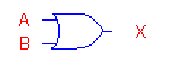
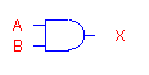
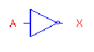
Figure 3. Logical Complementation (INVERTER) Gate
Schematic with its Truth-Table
These three logic functions are the basic building blocks of any
and all logic circuits possible. Any other logic function is
ALWAYS some combination of these three logic elements.
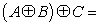
It is important to understand how to convert information from
a truth-table into a meaningful logic expression that represents
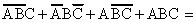
the truth-table exactly. As an example, let us use the truth-table
as given in figure 1. As you can see, this function is an "OR"
gate. As we already know, the Boolean Logic expression for an
OR gate is simply:
| (1.1) |
But how is this information determined from the truth-table of
figure 1 ? Well, let us reason the following. What does
the truth-table actually say "in English" ?
The output logic variable X will become a "1" whenever the system input conditions are satisfied. That is,
X = 1, whenever |
OR OR |
Figure 4. English Language interpretation of the
Truth-Table for an OR gate
Recalling that one of the so-called Boolean Algebra theorems says:
 (where K and 1 are logic inputs to
the system) What this actually says in "English" is
that "anything OR'd with "1" is "1".
The word "anything" indeed means anything, a single
logic variable or even a complex logic expression such as:
(where K and 1 are logic inputs to
the system) What this actually says in "English" is
that "anything OR'd with "1" is "1".
The word "anything" indeed means anything, a single
logic variable or even a complex logic expression such as:
|
| (1.2) |
Anything OR'd with "1" is ALWAYS equal to "1".
This is actually the most powerful and prevalent of all the Boolean
theorems used.
This theorem being true, one can simply write a phantom expression
and immediately know what that expression will evaluate to as
long as one of the terms in the logic expression is a "1".
That is: In general,
| (Logic expression #1)+(Logic expression #2)+(Logic expression #3)+( )+..+ 1= 1 | (1.3) |
Again, it does not matter what the logic expression is that is
enclosed within the parenthesis. Anything OR'd with "1"
is always equal to "1".
Let us now translate the English Language interpretation of the
OR function information found in figure 1 into a
Boolean Algebra logic expression.
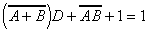
 ; Since, if
A = 0,
; Since, if
A = 0, must equal a "1"
| and B is given as "1" | |
| Therefore, "1" ANDed with "1" is equal to "1" (q.e.d.) |
 ;Since, if
B = 0,
;Since, if
B = 0,  must equal a "1"
| and A is given as "1" ; | |
| Therefore, "1" ANDed with "1" is equal to "1" (q.e.d.) |
 ;Since, if
A = 1 and B = 1, A ANDed with B = 1 (q.e.d.)
;Since, if
A = 1 and B = 1, A ANDed with B = 1 (q.e.d.)
This means that if any of the three logic expressions are "true"
or equal to a "1", the whole expression will evaluate
to a "1". Therefore the complete logic expression for
this truth-table can be written as:
| (1.4) |
But as we already know, this is the truth-table for a two input
OR gate with a logic expression of
| (1.5) |
These two expressions do not at first glance appear to be the
same ??? But are they ???
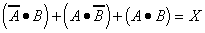
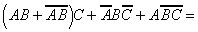
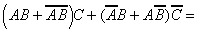
Let us now try to reduce equation 1.4 via Boolean algebra as follows.
For the sake of expediency, the "AND" dot will be left
out of any subsequent logic expressions.
| (1.6) |
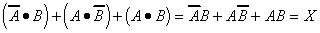
Factoring equation 1.6 yields
| (1.7) |
By Boolean theorem, "anything OR'd with its complement is
equal to 1, therefore:
| (1.8) |
and therefore
|
(1.9) | |
Equation 1.9 can also be reduced by Boolean theorem such that
|
(1.10) | |
Which is the result we expected.
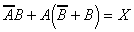
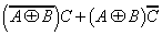
If one wanted to "add" another column to the truth-table(for
convenience), each component expression could be written adjacent
to the actual line that was affected as the following.
| . | |||
 | |||
 | |||
 |
As can be seen from figure 5, the logic expression for a given
truth-table can be written "directly" from the truth-table
as shown above. As a simpler example, this same technique could
have been applied to the AND function truth-table of figure 2.
This is shown below as
| . | |||
| . | |||
| . | |||
 |
As can easily be seen, this simple case does in fact yield the
logic expression for X as  with no factoring required. Note ! Simple truth-table component
expressions may not need factoring.
with no factoring required. Note ! Simple truth-table component
expressions may not need factoring.
Half Adders; Beginning the Picture
In order to understand how to add BCD numbers, the concept of adding binary numbers must first be understood. Whenever single digit numbers in any numbering system are added, the process that takes place is always the same. The two single digit numbers are added, in what ever system is being used, resulting in two results "always". These results are called the "sum" and the "carry".
"Most people tend to forget that there is a carry in
every addition even if the carry value happens to be zero."
The need to realize this stems from the fact that computers can
and will take nothing for granted as humans do. A carry of value
"0" must be used even if we as humans don't pay any
attention to it. Therefore, let us review the four possibilities
for adding binary numbers.
The basic (Algebraic - ADD) operation can be represented by the
following variables:
| (1.11) |
where
The four (algebraic addition) cases for binary numbers are shown
below in figure 7.
Remember !
*Although in base ten ( 110 plus 110
equals 210 with a zero carry ),
in base two (binary), 12 plus
12 = 102 , which means that 12
plus 12 = 0 with a carry of 1
To construct a logic system to produce these results would require
a system that has two inputs and two outputs as shown in figure
8 below.
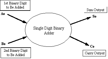
Understanding that there are actually two outputs
for an ADD function, one can now reconstruct the truth-table given
in figure 7 to include the "Boolean" logic component
expressions necessary to actually build this adder circuit.
| . | . | ||||||
 | . | ||||||
 | . | ||||||
| . |  |
Figure 9. Single-Digit Binary-Addition Truth-Table
with Sum and Carry Logic Expressions
Before actually constructing the logic circuit diagram, let us
look carefully at the logic expression for each output.
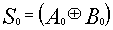
For the "Sum" output So;
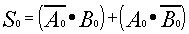 | (1.12) |
You may recognize this as simply the definition of an "exclusive
OR" function:
 | (1.13) |
For the "Carry" output Co;
 | (1.14) |
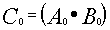
We can now see that this (Half-Adder) truth-table can be implemented
with just two logic gates, an Exclusive OR gate and an AND gate.
The actual circuit can be seen in figure 10 below.
Full Adders; Completing the Picture
The story of adding binary numbers is still incomplete. The case
arises when more than one binary digit is to be added to a similar
sized binary number such as the following.
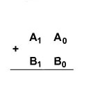
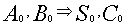
There are two binary numbers to be added. They are; A1
A0 and B1 B0
Applying the rules for adding single digits, we can proceed to add the "right most digits"- (LSB's) first. Note however that adding these digits; A0 to B0 yields a "sum" S0 and a "carry" C0
But now we are stuck with somewhat of a problem. The carry C0
now needs to be added to the two digits in the "next highest
place" as shown here.
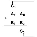
Figure 12 Sum and Carry Results of Adding the First-Place(LSB)
Digits of a Two Digit Binary Numbers
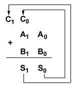
As can be seen in figure 12, there are now three digits to
be added together C0, A1 and B1,
not two as we have been shown how to do previously. What can
we do ???
The answer lies in building a "new" circuit that will
add three digits which we will call a "full adder".
Since we have no idea as to the values of each of these three
digit, we must account for every combination. As was done for
the half adder, a truth-table must be constructed demonstrating
all of the possible algebraic addition combinations for three
digits.
Something worth noting is that the sum of three digits will also
yield a "new" sum S1 and a "new"
carry C1 as shown in figure 13 below.
It goes without saying that this diagrammatic scheme can be extended
to any number of bits to be added. This will become important
to consider as we proceed with the topic of adding BCD digits.
A truth table can be constructed for adding 3 bits and is given
in figure 14 below.
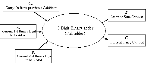
By using the same technique as we had done earlier, we can easily
observe that this logic system has three inputs and two outputs
and can be diagrammed as follows in figure 15.
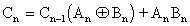
Designing the Full Adder Logic Circuit
At this point the technique for determining the actual logic circuit
should be very obvious. Using the same technique as was used
to design the Half Adder, we can now proceed with the design.
The truth-table representing the system can be reconstructed
with the appropriate logic expressions added to the lines whose
outputs are "1".
| . | . | |||||||||
 | . | |||||||||
 | . | |||||||||
| . |  | |||||||||
 | . | |||||||||
| . |  | |||||||||
| . |  | |||||||||
 |  |
|||||||||
Figure 16 Full Adder Truth-Table Showing Sum and
Carry Output Logic Expressions
As shown in this truth-table, there are two logic outputs, hence
two logic circuits to design. Let us attack this design by first
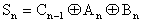
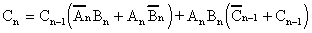
compiling the logic expressions for each output Sn
and Cn . As learned earlier each expression
can easily be written by simple inspection as;
 |
1.15 |
 | 1.16 | |
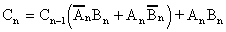
Equation 1.15 can now be examined. Upon examination, it can be
shown that this logic equation can be factored (actual factoring
is carried out in Appendix A) into the logic expression shown
below.
 |
1.17 |
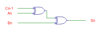
This "exclusive OR" equation is born out in the fact that if the truth-table of figure 16 is examined, it can easily be seen that a true "1" output for the "sum" Sn only occurs when there are an "odd number" of 1's being added. This is of course the definition of an exclusive-OR truth-table. Since there are three inputs, the expression given by equation 1.17 is justified. The logic circuit representing this expression is shown in figure 17 below.
Additionally, the logic expression of equation 1.16 can be reduced
by Boolean algebra as follows.
 |
1.18 |
 |
1.19 |
 |
1.20 |
Recognizing that 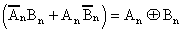 , equation 1.20 can
be re-written as
, equation 1.20 can
be re-written as
 |
1.21 |
The logic circuit shown in figure 17 can now be modified to accommodate
the addition of circuitry necessary to add the "carry"
Cn information. This addition is shown
in figure 18 below.
Keep in mind that there are other ways to have constructed this
"Full Adder". The factoring of equation 1.18 is not
limited to the example as given in this paper
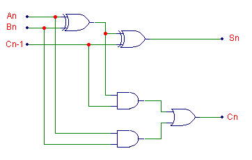
At this point, we have designed a "full adder" which
can be used to add any number of binary numbers. In fact, from
this point on, we will only use a "block diagram" representation
for a single digit adder. For example, the single digit adder
shown in figure 18 could be represented in block diagram fashion
as shown in figure 19. Additionally, groups of these can be "ganged"
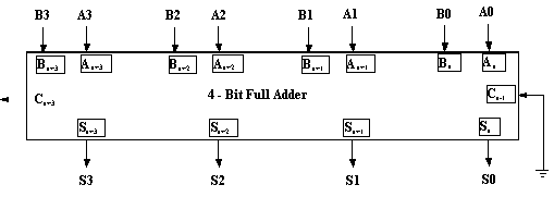
together to form "n-digit" full adders. Figure 20 shows
a 4 Bit(digit) full adder circuit.
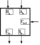
In fact, 4-Bit Full adders are quite common. So much so that
they can also be designated in block diagram fashion themselves.
A typical 4-bit Full Adder block diagram is shown in Figure 21
below.
We have now reached the point where we must explore Binary Coded
Decimal numbers or BCD for short. At this point however, it is
important to understand that the ONLY adders available to us for
use are "Binary Adders" as we have just discussed.
We will be implementing BCD adders using the only tools available
to us namely basic Binary-Full Adders.
Binary Coded Decimal numbers are actually binary numbers that
are "coded" to represent decimal numbers. In fact,
it is true that only numbers that come from well defined numbering
systems such as "Decimal,(base10)" , "Binary,(base
2)", "Octal,(base 8)", Hexadecimal,(base 16)",
etc. can be mathematically manipulated by addition, subtraction,
multiplication and division. Numbers not belonging to "actual"
numbering systems are not subject to the rules governing "real"
numbering systems. Coded numbers are "not real numbering
systems". In fact, they are just what they say they are,
"codes that represent actual numbers". Although the
actual numbers can be mathematically manipulated, codes follow
no such rules.
The intent here is to demonstrate an algorithm that can be used
to actually "add" BCD digits. The reason for the long
introduction into binary adders is the necessity for us to be
familiar with the only tool that is available to us for adding
any type of binary numbers.
Since BCD are codes that represent decimal numbers, let us determine
which decimal numbers are represented and by what codes. There
are ten distinct decimal characters in the decimal
numbering system. These are; 0, 1, 2, 3, 4, 5, 6, 7, 8 and 9
. Therefore, each of these must have a distinct code associated
with it. Since we are interested in coding these in a binary
fashion, it stands to reason that coding each as a binary number
makes sense. In fact, that is exactly what we will do. The following
table lists the ten decimal characters and their corresponding
BCD codes.
Since each BCD code must have the same number of bits to be consistent,
4 bits are used since the "largest" decimal number (9)
requires 4 bits, the rest of them must also be coded in 4 bits.
It is important, and I mean important, to understand that
a BCD number always, always, always contains 4 bits, no more and
no less. What about numbers larger than 9 ?? How are these represented?
They are represented or "coded" the same as a single
decimal digit. That is, each
decimal digit is coded "independently" with its corresponding
BCD single digit code. For example. The following are examples
of various decimal numbers that are coded as BCD.
| 6 | 0110 | |
| 49 | 0100 1001 | |
| 754 | 0111 0101 0100 | |
| 1058 | 0001 0000 0101 1000 | |
To further emphasize the relationship between Decimal and BCD,
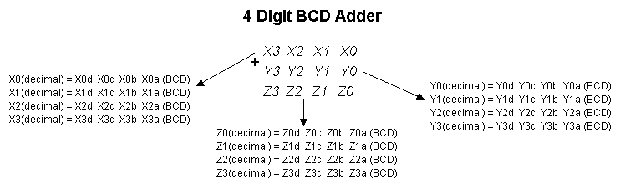
the following diagram is presented.
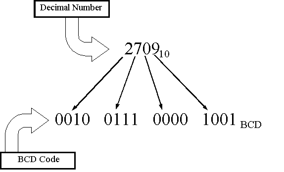
It should be noted that each individual decimal digit is represented
by its own BCD code. Each adjacent BCD digit-code has no relationship
with any other BCD digit code within the same decimal number.
In fact, the BCD code for the complete number given in Figure
23 is absolutely not the same thing as the binary number; 00100111000010012
. Do not confuse the two.

Figure 24 BCD Codes are NOT Equivalent to the Binary
Equivalent of the Decimal Number When Bits are Combined
as Shown Here
The binary equivalent of the decimal number 270910
is: 1010100101012
Now that we understand what BCD numbers are, let us proceed to
figure out a method to add them. Remember, the arithmetic "ADD"
operation works normally on "real numbering systems only".
We want to create a method to add codes and come out with the
correct answer in the same coded system(BCD).
Let us now examine some examples of several additions of single-digit
decimal numbers and the equivalent operation using Binary and
the expected result using BCD.
| 1 + 0 = 1 | 00012
00002 00012 | 0001BCD
0000BCD 0001BCD | ||
| 1 + 1 = 2 | 00012
00012 00102 | 0001BCD
0001BCD 0010BCD | ||
| 1 + 2 = 3 | 00012
00102 00112 | 0001BCD
0010BCD 0011BCD | ||
| 1 + 3 = 4 | 00012
00112 01002 | 0001BCD
0011BCD 0100BCD | ||
| 1 + 4 = 5 | 00012
01002 01012 | 0001BCD
0100BCD 0101BCD | ||
| 1 + 5 = 6 | 00012
01012 01102 | 0001BCD
0101BCD 0110BCD | ||
| 1 + 6 = 7 | 00012
01102 01112 | 0001BCD
0110BCD 0111BCD | ||
| 1 + 7 = 8 | 00012
01112 10002 | 0001BCD
0111BCD 1000BCD | ||
| 1 + 8 = 9 | 00012
10002 10012 | 0001BCD
1000BCD 1001BCD | ||
| 1 + 9 = 10 | 00012
10012 10102 | 0000 0001BCD
0000 1001BCD 0001 0000BCD | ||
| 2 + 9 = 11 | 00102
10012 10112 | 0000 0010BCD
0000 1001BCD 0001 0001BCD | ||
| 3 + 9 = 12 | 00112
10012 11002 | 0000 0011BCD
0000 1001BCD 0001 0010BCD | ||
Figure 25 Comparison of Adding Single Digit Decimal
Numbers to Adding their Binary Equivalents to What the Results
Should be if BCD Digits Could Be Added
Comparing the columns of the table of figure 25, several observations
can be made. The first is that the difference(
) between the "Binary Answer" and the "BCD
Answer", to the various addition examples, is zero
when the answer to the addition is contained in 4-bits and
the largest BCD single digit number does not exceed the equivalent
of the decimal number 910 . Remember, BCD digits are
binary codes that represent single digit decimal numbers from
010 to 910 only.
Something happens, however, when the result of the addition is
greater than 910 . It is this result that is the most
interesting and will be explored here.
The range of single digit sums given in figure 25 can be expanded
to show the absolute largest result possible. This would be when
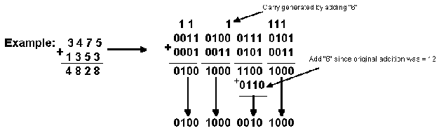
910 is added to 910 resulting in 1810.
This "the largest possible result of adding two single digit
decimal numbers" is shown in figure 26 below.
| 9 + 9 = 18 | 10012
10012 100102 | 0000 1001BCD
0000 1001BCD 0001 1000BCD | ||
Notice that there is a delta difference( ) of 6 listed
in the table of figure 25 where the answer is greater than 910
or 10012 . How is this difference calculated ? Where
does this delta come from?
The first thing to realize is that the only tool we have for adding
any type of binary related numbers is "the full adder".
This full adder tool would yield the correct "binary"
result but certainly not the BCD results as shown in figures
25 and 26 corresponding to the rows where the delta was labeled
as 6.
Since the result of a mathematical ADD operation is conducted
in a "full adder", the result will be in straight binary.
The user, however, would like the answer to be in BCD code.
Therefore, there needs to be a "middle-man" operation
that will "look" at the resultant binary number and
determine whether this code needs to be adjusted to meet the BCD
code output criteria.
Looking at the results of figure 26, one can observe that the
result of an ADDITION operation resulted in the full adder's output
being
which is the correct binary result of adding 910
and 910 or 10012 and 10012
. But what we actually want to appear at the output of the full
adder is the following.
This output Result 2. can be interpreted by an observer as BCD
by simply dividing up this Result 2. number into 4-bit nibbles
starting from the LSB which would yield the following.
As you can see, this is indeed the BCD code for 1810
This gets us back to the delta. Just what is it? Since there
are now two binary results to the addition of 910
and 910 , the real binary solution given as Result
1. and the binary solution that we would like, given as Result
2. we must build a translator circuit that can convert
Result 1. into Result 2. Upon observation of a comparison of
various examples as given in figures 25 and 26, one can observe
that the "difference" between Result 2. and Result 1.
for any summed answer greater than 9 (for any combination of single
digit decimal numbers to be added) is always equal to 6. That
is (Result 2. - Result 1. ) = 6 This is
seen here is Figure 27.
|
|
|
|
|
| 10102 | 0001 00002 | 0001 0000BCD | ||
| 10112 | 0001 00012 | 0001 0001BCD | ||
| 11002 | 0001 00102 | 0001 0010BCD | ||
| 11012 | 0001 00112 | 0001 0011BCD | ||
| 11102 | 0001 01002 | 0001 0100BCD | ||
| 11112 | 0001 01012 | 0001 0101BCD | ||
| 100002 | 0001 01102 | 0001 0110BCD | ||
| 100012 | 0001 01112 | 0001 0111BCD | ||
| 100102 | 0001 10002 | 0001 1000BCD |
Defining a Rule for BCD Addition
Upon observation of the previous information, a rule can be asserted
to convert summed outputs from a full adder into proper BCD code.
The rule is the following:
This aforementioned rule is always true. However, as a
practical matter, there is a caveat to this scenario.
Since Full Adders are to be used to add binary numbers, consideration
must be given to a method of determining whether a resultant sum
is actually greater than 9.
Since adding single decimal digits is the same as adding two 4-bit
binary numbers, summed results could range from 0000 to 10010,
which is of course 010 to 1810. Care must
be taken when trying to detect for numbers greater than 9, specifically
summed results such as 16 whose binary value is 1 00002
. In the case of the number 16, if a single 4-bit full adder
is to be used, the four LSBs will be equal to zero but there will
be a "carry" 5th bit generated to the next(if available
4-bit full adder stage).
One could certainly break this detection problem down into two
pieces. That is, one could monitor the 4 LSBs of the Full Adder
and determine when the value that appears on these 4 lines is
greater than 9 i.e. 10 to 15. If this is true, than add 6 to
this result as stated in the rule. Also, if these four LSBs
are less than 9 and there is a carry out of the MSB, as is the
case for the number 16, add 6. In either case, we have added
6 for any summed result greater than 9.
Implementing a Simple BCD Single Digit Adder
Implementing a single digit BCD adder is not that difficult when
one understands the rule and the concept of Full Adders. Remember,
adding two single digit BCD numbers is the same as adding two
binary numbers with the exception that the only allowable input
numbers range from 0 to 9. This is actually quite nice since double
digit numbers are not allowed as BCD coded numbers. The following
figure is a basic Full Adder that can easily add two single digit
decimal numbers from 0 to 9. This can be written as:
| A3 A2 A1 A0 | |
| + | |
| B3 B2 B1 B0 |
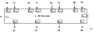
The detection circuit for numbers greater than nine must now be
designed and added to this existing full adder.
This as any other design starts with a truth-table. Let us start
by designing a detection circuit for 4-bit numbers greater that
910 or 10012.
| . | . | |||||
| . | . | |||||
| . | . | |||||
| . | . | |||||
| . | . | |||||
| . | . | |||||
| . | . | |||||
| . | . | |||||
| . | . | |||||
| . | . | |||||
 |
||||||
 |
||||||
 |
||||||
 |
||||||
 |
||||||
 |
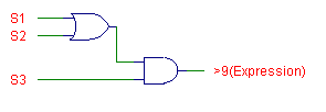
Solving this truth-table for >9(Expression) gives
the following Boolean reduction equations.
>9(Expression) =
 | 1.22 |
Combining terms gives
|
1.23 | |
Since 
>9(Expression) =
 |
1.24 | |
Further factoring yields
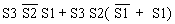 |
1.25 | |
But 
>9(Expression) = 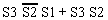
| 1.26 | |
Factoring again yields
 |
1.27 | |
Finally factoring yields
 |
1.28 | |
giving the final result as:
>9(Expression) = 
| 1.29 | |
Alternately this expression could be written as
>9(Expression) = 
| 1.30 | |
Either one is correct. Each actual implementation is slightly
different. Either of the following circuits can be constructed
to detect 4-bit summed numbers greater than 9.
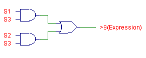
|
|
Figure 30 Two Different Circuit Implementations to
Detect Full Adder Outputs Greater than 9
Now that a circuit has been developed to allow us to detect 4-bit
numbers greater than 9, let us reiterate just what we must do
to add two single digit BCD digits.
That's all there is to it. Let us now implement the circuit to
perform this BCD addition.
** A carry out will occur in all cases where the original sum was equal to 1610, 1 00002, which is itself greater than 9, or after "6" has been added to the original sum that was found to be greater than 9.
In order to implement this "complete" BCD" adder,
it should first be understood that the implication of adding an
addition "6" requires an additional Full Adder. The
following logic circuit of figure 31 is proposed for this purpose.
Note that this circuit fulfills all of the requirements mentioned
earlier. Try it you'll like it !!!
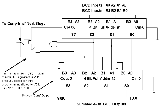
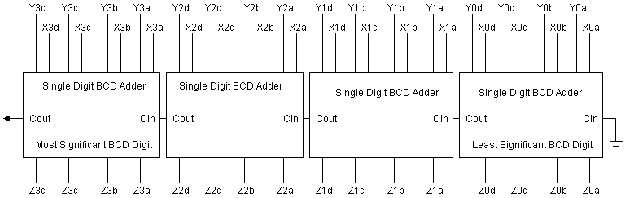
Additionally, BCD adders can be constructed for more than just
single digits. This is the case as shown in figure 32. The basic
single digit BCD adder has been reduced to a single block diagram
and "cascaded" with four other single-digit BCD adders.
The diagram is self explanatory.
Designing and implementing BCD adders is a rather simple task
but does require the designer to have thorough knowledge of Full
Adders along with the understanding of the concept behind the
creation of BCD number codes themselves.
1. Digital Electronics 3E, Kleitz, William, Prentice
Hall,1993, ISBN 0-13-210378-8
2. Digital Systems, Principles and Applications 5E,
Tocci, Ronald, Prentice Hall, 1991, ISBN 0-13-213224-9
3. Practical Digital Design Using ICs 3E, Greenfield,
Joseph D., Prentice Hall, 1994, ISBN 0-13-689894-7
4. Digital Design Fundamentals 2E, Breeding, Kenneth
J., Prentice Hall, 1992, ISBN 0-13-211277-9
5. Computer Engineering Hardware Design, Mano, Morris,
Prentice Hall, 1988, ISBN 0-13-162926-3
6. Digital Logic and Computer Design, Mano, Morris
M., Prentice Hall, 1979, ISBN 0-13-214510-3
7. Digital Design Principle & Practices 2E,
Wakerly, John F., Prentice Hall, 1994, ISBN 0-13-211459-3
The following Boolean reduction will show that
| A.1 |
is true.
|
A.2 | |
|
A.3 | |
|
A.4 | |
|
A.5 | |
Let 
Re-writing equation A.5 gives
|
A.6 | |
which is the Boolean equivalent of an Exclusive OR of the form
|
A.7 | |
Substituting back for X yields
|
A.8 | |
|
A.9 | |
q.e.d.