by
Ahmad Zargari, Assistant Professor
Michael Combs, Graduate Assistant
Morehead State University
Introduction
In today's technology-driven society, microprocessors and microcomputers are an integral part of peoples' lives. The applications of microprocessors are almost endless. Because of microprocessor technology, just about any electronics or electrom echanical device is a candidate for automatic control. We wake up to a microprocessor-controlled alarm clock, read a newspaper that was edited by a microprocessor-based word processor, and watch the morning news on television as a microprocessor fine-tun es the picture (Goody 1993). One of the most common uses for microprocessors is in personal computers.
An ever-increasing demand for microprocessors in industrial, educational, and business organizations mandates that all students in the field of electronics be provided with a basic knowledge of microprocessor technology and its applications. The rapi d advancement of computers into our everyday affairs has created society's need for individuals who are able to understand the fundamental concepts and applications of microprocessors. In order to provide electronics students with an opportunity to devel op an understanding of microprocessors, this project has been included in the senior-level course, Computer Electronics - EET 445. In this course, students build an 8088-based single board microcontroller as a major project. Using Fuller's Build Your Own Computer Lab Manual, students first construct and test the basic circuit for the 8088 controller. Then, additional components are added to improve the microcomputer's functionality and to provide students with practical experience in interfacing techniques.
We selected the Intel 8088 microprocessor because it has relatively higher execution speed, larger memory size, and additional instructions, which provides students with a practical knowledge of microcontroller technology. The IBM personal computer, w hich came out in mid-1981, was one of the earliest microcomputers to utilize a 16-bit microprocessor, the 8088, as its central processing unit (Triebel & Singh 1997). Through the construction process, students gain knowledge and experience in circuit des ign, wire-wrapping and soldering techniques, board design and parts layout, static and dynamic testing, programming, use of test equipment for analysis and troubleshooting, and data acquisition. Upon completion of the project, the student will have const ructed a fully functional single board microcomputer with a 64K memory, a printer port, two serial ports, an analog-to-digital converter, and over 28 parallel input/output (I/O) lines. The project is organized around the following 12 steps:
Step 1: The Voltage Regulator Circuit
Power is supplied to the microcontroller through a 9 Volt DC (VDC) power supply. Power form the 9 Volt DC power supply is applied to a voltage regulator circuit that steps the voltage down to 5 Volts DC. This circuit is fairly simple to build because the support circuitry for the LM7805 (5-Volt voltage regulator IC) requires very few components. The circuit consists of an input jack, a power switch, a resistor, one LED, a voltage regulator IC, and two capacitors. The 9 VDC is brought in through the input jack and then routed to a double pole double throw switch (DPDT). This switch is used to turn the power to the microcontroller on and off. The reason for using the DPDT switch is to allow for disconnecting both the hot and neutral lines. The LED is used to indicate whether power to the circuit is on or off. The tantalum capacitors are used to filter the input and output voltages of the 5 VDC regulator. The student uses basic soldering skills to build the circuit. Once the circuit is completed the student uses a multimeter to do a resistance test to check for cold solder joints or short circuits.
Once this testing is completed, power is applied to the circuit. The student then checks the voltage regulator for overheating. A multimeter is used to check the final output voltage of the circuit. The desired voltage is between 4.85 VDC and 5.15 V DC. The output voltage for this circuit is 4.92 VDC. Once the circuit has been properly examined and tested, the student is ready to move on. The next step is to distribute power to all ICs in the microcontroller. Figure 1 displays the voltage divider circuit.
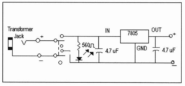
Figure 1. The Voltage Regulator Circuit
Step 2: The Power Bus
With the completion of the power circuit, power is now ready to be connected to the various devices in the microcontroller. IC wire wrap sockets are now placed on the protoboard. Once the IC sockets are laid out and fastened to the board power lines, they are ready to be connected. One capacitor is soldered from Vcc to Ground on each chip that has 24 or more pins and one capacitor is soldered from the Vcc wire on the bus to the Ground wire on the bus for every two chips that have less than 24 pins. Ceramic disk capacitors are used to protect the ICs from power spikes, which can damage the ICs. Once the power bus is soldered together and tested for shorts and other wiring errors, connections are soldered to the power supply circuit. The voltage acr oss each socket is tested individually. The voltage across each socket should be the same as the supply voltage. In this exercise, the wire-wrap sockets for the various chips are laid out on the circuit board and labeled. Red hookup wire is run to the Vcc pin of each socket. Black hookup wire is run to the ground pins of each socket. The voltage connections are soldered and .01-microfarad de-spiking capacitors are added to the circuit. Figure 2 displays the component layout.
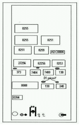
Figure 2. The Components Layout
Step 3: Wire-wrap Technique and Practice
To make wire-wrap connections, one inch of insulation must be stripped from the wrapping wire using the built-in stripper. The wire must then be inserted into the wrap slit of the tool along with 1/8 of an inch of the insulation. A 90-degree bend is then made in the wire at the base of the tool and the tool is placed over the wire-wrap post and pushed down as far as it will go. While holding the wire steady with one hand, the tool is turned clock-wise, using even pressure, until all of the wire in t he tool is around the wire-wrap post. The connection should have approximately 1½ turns of insulation around the base of the connection for strain relief and approximately 8 to 10 turns of bare wire wrapped tightly together around the post. Wire-wrap te chnique is illustrated in Figure 3.
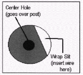
Figure 3. Wire Wrap Techniques
Using the wire wrap technique, the student will continue wiring with the next circuit. The next step is the construction of the clock circuit.
Step 4: The 8088 Clock Circuit
The clock circuit provides the clock signal to the microprocessor, provides the READY input to the microprocessor, and provides the peripheral clock and reset circuitry to the rest of the circuits as the time base. The 8284 IC takes the time base (15 MHz) and divides it internally by three to generate a 5 MHz clock (CLK) signal. The signal is also divided by a factor of six to generate the PCLK or peripheral clock output of 2.5 MHz. A m omentary contact normally open push-button switch is connected to the reset (RES) pin of the 8284 IC chip and to ground to provide the manual reset. When the RES pin goes to ground, the internal reset mechanism of the chip is started and this provides a dependable and orderly sequence that resets the rest of the computer. The circuit also provides a power on reset by the use of an RC circuit connected to the RES pin that slowly raises the pin from logical zero to logical one, imitating the manual reset each time the computer is started. The circuit is wired and the power bus connections are checked without the chip installed and then with the chip installed. An oscilloscope is then hooked to the CLK output and the waveform is observed to make certain that the output is a 5-MHZ square wave. The OSC output is checked next. It should be the same as the input from the crystal, 15 MHz. The PCLK output is then tested to see if it is 2.5 MHz. Finally, the waveform across the crystal is observed. Figure 4 illustrates the 8088 clock circuit. In the next step, the 8088 microprocessor IC is installed.
Figure 4. The 8088 Clock Circuit
Step 5: The 8088 Microprocessor Installation
The actual microprocessor is installed and tested in this exercise. The TEST switch and related de-bouncing circuitry are installed. The microprocessor is installed in this circuit in the Minimum mode and with the DMA controller disabled. This makes the data connection scheme much simpler, since it allows the data and address pins to be connected directly to the data and address busses without any support circuitry. A de-bounced switch circuit (two 74LS00 NAND latches) is put together and connected to the TEST pin. Th is switch circuit will be used to control the execution of test programs. Once the circuit is built, the voltages are checked and testing is done on the latch. At the power on condition, the correct logic level at the TEST pin is 1. The logic level sho uld go from 1 to 0 when the switch is toggled. Figure 5 displays the de-bouncer switch circuit. In the next step, the memory circuit is constructed.
Figure 5. The De-bouncer Circuit
Step 6. The Memory Circuit
In step 6, the RAM and EEPROM are installed and tested. The address latch is installed and tested. The control bus decoder is installed and tested. The 74LS138-control bus decoder is a 3-to-8 decoder that is wired to the RD, WR, and IO/M on the 8088
microprocessor, and is used to partially encode the control bus of the 8088 microprocessor. The 74LS373 address latch is used to capture address information from the low-order byte of the Address/Data bus. The memory consists of 32 K of EEPROM and 32 K
of RAM. The RAM occupies address ranging from 0000H to 7FFFH and the EEPROM occupies the address range 8000H - FFFFH. The addition of an inverter circuit allows switching between EEPROM and RAM. After the circuit is wired and tested electrically, a te
st program is burned into the EEPROM to put the computer into a loop so that output on the IO/M line can be checked. When the program is running the output constantly changes logic levels, but when the toggle switch is off the output stays at logical 0.
As long as the program runs correctly, the circuit is properly wired. Figure 6 displays the memory circuit. In step 7, the programmable timer circuit will be installed.
Figure 6. The Memory Circuit
Step 7. The Programmable Timer Circuit
The I/O decoder is installed in this exercise. The 8253/54 PIT (programmable interval timer), which is used to generate the timing signals to the peripheral I/O devices is installed. In the PC there is a single clock used to synchronize activities of all peripherals chips connected to the CPU. The clock, which has the highest frequency in the system, belongs to the 80x86 CPU Family. There are functions within the PC that require a clock with a lower frequency. The 8253 is used to drop the frequenc y to the desired level for various applications such as the beep a sound in the PC (Mazidi & Mazidi, 1993). The 74LS138 is a 3-to-8 decoder used to decode signals on the high-level address bus and select the proper I/O device for the microprocessor to ac cess. It does this by taking the high level address and converting it to one of 8 inverting outputs connected to the chip select on each I/O device in the circuit. The 8253 is used as a baud rate generator. It sends the proper frequency square wave to t he 8251A to make it a 9600 baud serial port. The circuits are wired and checked electrically and then a program is loaded into the EEPROM and the computer is started. The OUT pin is tested with an oscilloscope to be certain that the output frequency is 500 KHz.
Step 8: The 8255A Parallel I/O Port
The parallel I/O circuit is installed in this part of the project. The 8255 chip is a widely used I/O chip. It is designed for both memory-mapped and peripheral I/O. The 8255 is in a 40-pin DIP chip arrangement. It has three separately accessible p orts, A, B, and C, this makes it much more economical than the 74LS244 and 74LS373 for I/O ports (Mazidi, Mazidi 1993). These ports can be programmed for either input or output and are used to interface the 8088 with different devices. Two 8255A chips a re used in this computer. One is used as the printer interface and one is used to handle all other parallel I/O activities. The circuit is constructed and tested electrically without any chips installed; then, with all of the chips installed. A static test is done by putting a logic probe on the RESET pin of the 8255A and pressing the system reset button. When the button is pressed, the pin should go from logical 0 to logical 1. When the button is released, the pin should go from 1 back to 0. A test program is then loaded into EEPROM that configures the parallel ports and sends all 0?s and then all 1?s to them. The circuit is correct when a continuous ON-OFF-ON-OFF pattern is read at each bit of each port.
Step 9: The 8259 Interrupt Controller
The interrupt controller is installed and tested in this exercise. Hardware interrupt theory is discussed. The 8259 handles all of the hardware interrupts in the computer circuit. It also allows for enabling and disabling of any interrupt via softwa re. The chip is connected to the data bus, the interrupt lines of the peripherals, and the low-level address line. When an interrupt request is sent to the 8259 by one of the other chips, an interrupt request is sent to the 8088 via the INTR line. The 8088 then acknowledges the request via the INTA line. The type of interrupt is then communicated to the 8088 and the proper routine is executed.
The circuit is wired and tested electrically. A test program is loaded into the EEPROM that sets up a dummy service routine and waits for an interrupt. The NAND latch is used to simulate an interrupt request. Once the request is generated the program goes into an endless loop and pulses the I/O lines on the 8255 port B. I f the port pulses, the circuit works.
Step 10: The Serial I/O Circuit
The primary serial I/O port is installed and tested in this section of the project. Serial communication in microcomputer circuits is discussed. This computer uses the 8251A Universal Synchronous/Asynchronous Receiver-Transmitter (USART) to handle se
rial communication. The 8251A is essentially a parallel-to-serial/serial-to-parallel converter that can be in either asynchronous or synchronous environments. It is programmable to fit a wide range of related applications (Goody, 1993). The USART is co
nnected to the data bus where it takes an 8-bit data word and transmits it one bit at a time over a single wire at a predetermined clock speed called a baud rate. It receives data over a single wire, converting it back into 8-bit words for transmission o
ver the data bus. The 8251A interface is interrupt driven so that the 8251A and the 8088 only talk when there is actual data to be transmitted or received. First, the circuit is wired and tested electrically. The MONITOR program is then loaded into the
EEPROM and the computer is connected to a personal computer via serial ports for testing. The microcomputer is switched on and some characters are typed on the PC keyboard. If the keys are echoed by the microcomputer, the program and the circuit are op
erating properly. Figure 7 displays the serial I/O circuit.
Figure 7. The Serial I/O Circuit
Step 11. The Monitor Program
The MONITOR program is discussed in detail in this exercise. The TERM88 program that interfaces the microcomputer to a PC is also discussed. The monitor program is designed to allow the user to manipulate and examine all functions of the microcompute r. It contains machine language routines to allow the user to examine memory locations, move blocks of memory, read and write to a device in the computer, change memory contents, etc. The TERM88 program acts as a terminal interface between the microcomp uter and the personal computer. It allows the user to download files to the microcomputer, look at the microcomputer' s screen buffer, and take snapshots of the screen buffer and switch COM ports.
Step 12. Simple Parallel I/O using the 8255A
The simple I/O interfacing method is discussed. The auxiliary parallel I/O circuit and the LED display are installed. The simple I/O method of interfacing calls for all input and output to happen at specific times in the execution of a program as determined by software and not hardware interrupts. First, the LEDs and limiting resistors are installed. Then the DIP switches are installed along with the pull up resistors. The LED portion of the circuit is wired to the 74LS240 and the DIP switches are wired to the parallel port A of the 8255. The connections are checked electrically and then the monitor program is used to se nd configuration information to the 8255 and sample data is inputted and outputted using the switches and LEDs. Figure 8 illustrates the parallel I/O circuit.
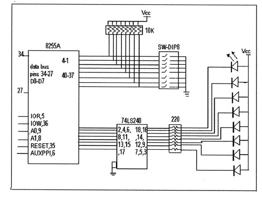
Figure 8. Parallel I/O Circuit
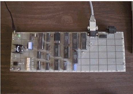
With the wiring of the parallel I/O circuit using 8255A, the hardware part is completed. The completed circuit board is shown in Figure 12.2.
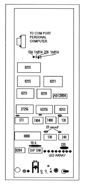
Figure 9. The Completed Board
Conclusions
This project enables students to develop advanced technical skills that are essential to function in today's electronics field. It helps the participants to build upon their electronics knowledge and become more proficient in the field of microproces sor technology. Our preliminary assessment indicates that although the project is challenging for students it is not overwhelming or beyond their capabilities. It has helped students to develop practical troubleshooting and problem-solving experiences r equired for testing, troubleshooting, and resolving problems. The microprocessor project has helped to demystify the inter workings of microcontroller technology and has generated and enhanced students' interests in further developing and exploring their understanding of microprocessors. The sense of self-satisfaction displayed by students upon completion of this project is conveyed by their positive attitudes toward their class work. There is only so much that can be learned in the classroom; this pro ject compliments that very well.
References
Fuller, W. (1995). Build your own computer. New York, NY: Delmar Publishers Inc.
Goody, R. (1993). Intel Microprocessors: Hardware, Software and Applications Westerville, OH: Glencoe Division of Macmillan/Mcgraw-Hill.
Mazidi, M., and Mazidi, J. (1998) The 80x86 IBM PC and Compatible Computers (Volume II): Design and Interfacing of the IBM PC, PS, and Compatibles Upper Saddle River, NJ: Prentice-Hall.
Subbarao, W. V. (1992). The 8086/8088 family of microprocessors. New York, NY: Delmar Publishers Inc.
Triebe, W., Singh, A. (1997).The 8088 and 8086 Microprocessors: Programming, Interfacing, Software, Hardware, and Applications Upper Saddle River, NJ: Prentice-Hall.