| William B. Hudson hudson@eece.ksu.edu Department of Electrical and Computer Engineering Kansas State University |
Jeffrey S. Beasley
jbeasley@nmsu.edu Department of Engineering Technology New Mexico State University |
Abstract
Mixed logic notation provides a simplified mechanism for the analysis and design of digital circuits. Correct use of mixed logic notation provides logic expressions and logic diagrams that are analogs of each other. Additionally, a mixed logic diagram provides clear documentation as to the operation of a circuit. Even though mixed logic techniques are easily understood, the positive/negative logic techniques are more prevalent in digital textbooks. Adding to the confusion and the misconceptions concerning mixed logic is the fact that almost all data books refer to logic gates in terms of "Positive Logic" functionality [1,2]. The gate symbols provided in data books typically show only the positive logic functionality of the logic gate. A demonstration of this fact is the description of the 74LS00, as provided by Texas Instruments, in the TTL Logic Databook [3]. The positive logic interpretation of the "NAND" gate is that it will output a "low" logic level given two high inputs. That is, if A is high "AND" B is high the output will be low. An equally correct interpretation of the operation of this gate would be if A is low "OR" B is low, the output will be high. Those individuals trained in mixed logic realize that the 74LS00 device can also be viewed as either an "AND" or an "OR" operation. By viewing both the "AND" and "OR" functionality associated with each logic gate it becomes easy to design and analyze digital circuits.
When using mixed logic, it is possible to view truth tables in a more general way, than is possible with positive logic. In positive logic, the basic building blocks are viewed as being the "AND", "NAND", "NOR", "OR" and the "Inverter."[4] The "Exclusive OR" can be obtained from a combination of "AND", "OR" and "Inverter" operations. The truth tables associated with the "AND" and "NAND" positive logic operations are provided in Tables 1 and 2 to help demonstrate the difference in the positive logic and mixed logic "one" and "zero" notation.
| A | B | C |
|---|---|---|
| 0 | 0 | 0 |
| 0 | 1 | 0 |
| 1 | 0 | 0 |
| 1 | 1 | 1 |
| A | B | C |
|---|---|---|
| 0 | 0 | 1 |
| 0 | 1 | 1 |
| 1 | 0 | 1 |
| 1 | 1 | 0 |
Mixed logic does not restrict a "1" to always represent a high and a "0" to always represent a low. It is important to note that in positive logic, a "1" is always considered a logic high and a "0" is always a logic low. The mixed logic interpretation of these functions is a more general interpretation than the positive logic interpretation. The truth tables associated with the mixed logic "AND" and "NAND" are shown in Tables 3 and 4.
| A | B | C |
|---|---|---|
| 0 | 0 | 0 |
| 0 | 1 | 0 |
| 1 | 0 | 0 |
| 1 | 1 | 1 |
| A | B | C |
|---|---|---|
| 0 | 0 | 0 |
| 0 | 1 | 0 |
| 1 | 0 | 0 |
| 1 | 1 | 1 |
The generality of the mixed logic approach allows all "AND" operations, regardless of input and output, assertion levels to be represented by a single truth table. The same generalization applies to the "OR" function. The general notational technique used in mixed logic makes it possible to easily visualize "AND" and "OR" operations.
Concept: The correct use of mixed logic requires the placement of the "AND" or "OR" symbol in the logic diagram anytime an "AND" or "OR" operator is called for in the Boolean Expression. The voltage requirements are met by the assignment of assertion levels.
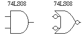
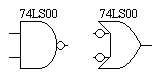
To clearly denote, "AND" and "OR", operations on a logic diagram, alternate symbols have been developed. The basic positive logic symbols for the "NAND", "AND", "OR" and inverter operators are shown in Figures 1 through 5.
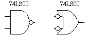
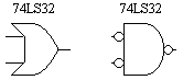
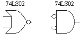
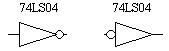
Shown with each positive logic symbol is an equivalent logic symbol. The
equivalent logic symbol is obtained by changing the operation, "AND" to "OR" or
"OR" to "AND" and complementing assertion levels. The circle, or "bubble" on the
output of the "AND" gate in Fig. 2 tells us the output will be low when asserted.
The absence of bubbles on the inputs tells us that both of the gate inputs
require a logic high to be asserted. The mixed logic interpretation for the
logical "AND" circuit shown in Fig. 2, is given by the expression F =
(A.B)-L This expression is much clearer than the
positive logic expression since
since can also be interpreted as
  . Many digital logic textbooks
demonstrate the equivalence of the alternate symbols available for the various
positive logic functions [4,5,6,7,8,9,10,11] however, not all of the textbooks
fully utilize mixed logic for design and documentation to best display the
intended function.
. Many digital logic textbooks
demonstrate the equivalence of the alternate symbols available for the various
positive logic functions [4,5,6,7,8,9,10,11] however, not all of the textbooks
fully utilize mixed logic for design and documentation to best display the
intended function.
The ability to freely convert "AND" and "OR" symbols makes it possible to
easily realize circuits given descriptions of the circuit operation. Further by
conversion of gate symbols the operation of the circuit is always clearly
communicated by the logic diagram. The following example, using mixed logic
symbology, demonstrates logic realization with both "AND" and "OR" logic
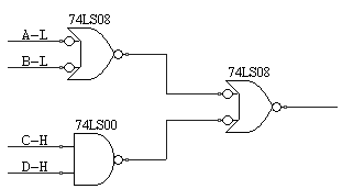
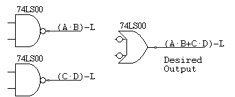
operations. The problem description requires a circuit which produces a logic
high output signal when inputs A "AND" C are low "OR" B is high. Two circuits
using mixed logic notation are provided in Figures 6(a) and 6(b) which meet the
problem statement.
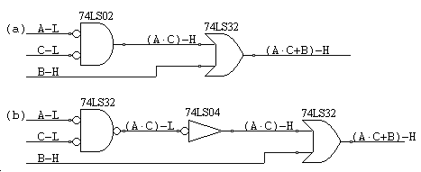
Concept: The mixed logic design approach allows the freedom to produce circuits that generate and respond to either high or low logic levels.
In terms of the logic diagram, a bubble on the output shows that a low will be produced when the gate conditions are met. To further emphasize this point, the logic expression at the gate output should contain -L (i.e. F = (A.B)-L) at the end of the expression. Likewise, if meeting the gate conditions results in a logic high output, the output expression should be labeled with a -H (i.e. F = (A.B)-H). This notation is shown in Figures 6(a) and 6(b).
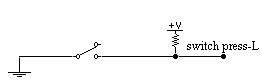
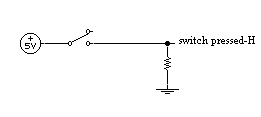
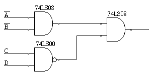
In mixed logic, the input and output voltage levels requirements are expressed in terms of their assertion levels. For example, a positive logic NAND gate is expressed as being an "AND" function with an "asserted low" output and "asserted high" inputs. Assertion is a word which when used in the digital sense means "the affirmative position of an action related to a Boolean variable." This concept is demonstrated with the circuits shown in Figures 7 and 8.
Let's assume that the switches, shown in Figures 7 and 8, are spring loaded
so that in order for contact to be made they must be pressed.
Easy interpretation of a circuits operation is possible by maintaining the
consistent use of assertion levels. An example is provided using the circuit
shown in Fig. 9.
Concept: A conflict in mixed logic notation is used to denote that a mismatch of assertion levels is present in the circuit.
The conflicted condition is indicated by placing a dot over the input of the conflicted node. Not all mixed logic textbooks use the dot to indicate a conflict. Some textbooks also differentiate between conflicts in "AND" and "OR" logic operations. However, the authors have found that using only the dot is most useful. When a conflict is found, an overbar is added to the logic expression for the particular variable(s) and the affected term(s) are read as being "not asserted." The example of this notation is shown in Fig. 11.
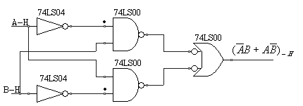
As shown, the conflict is denoted with a "dot" and an overbar is placed in the equation over the affected variable. The resulting output expression is understood to mean if A is not asserted "AND" B is asserted "OR" A is asserted and "B" is not asserted the output will be asserted. Inspection of the output assertion level in the circuit diagram shows that the output will be a logic high when asserted. Examination of input signal assertion levels show that A and B inputs will be a logic high when asserted.
Concept: A change in assertion level is sometimes required to avoid or create a conflicted condition in the design. This is accomplished by using an inverter.
Notice that the "bubble is located on the output for Fig. 12(a) yet it is on
the input for Fig. 12(b).

The mixed logic expression realized from the circuit shown in Fig. 13 is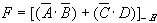 . None of the barred expressions result from the inverter,
rather they are a result of conflicts on the inputs of other circuit
elements.
. None of the barred expressions result from the inverter,
rather they are a result of conflicts on the inputs of other circuit
elements.
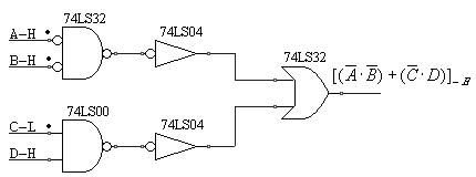
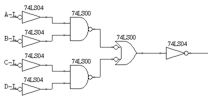
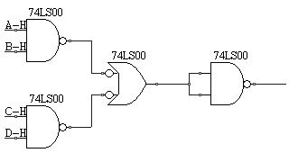
Concept: Mixed logic notations allow for the easy implementation of logic circuit functions from a limited parts supply.
Frequently it becomes necessary to design circuits from a restricted set of
devices, either to minimize parts count or because of limited availability of
alternate devices. The use of mixed logic allows this to occur naturally. For
example, if the expression F =
[(A.B)+(C.D)]-L is required (with all
inputs asserted low) and only 74LS00 and 74LS04 devices are available, mixed
logic allows rapid circuit design. The first step is to draw the gates and their
alternate (complementary) representations as shown in Fig. 14.

Connection of devices is accomplished by keeping track of the assertion levels
and avoiding mismatches. Inverters should be added, where needed, to establish
appropriate assertion levels. The completed circuit is shown in Fig.
17.
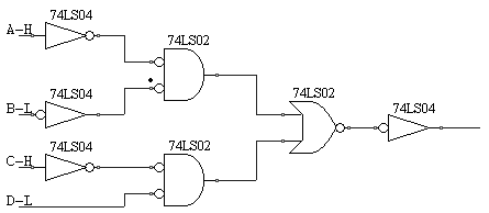
The same expression F = [(A.B) + (C.D)]-L will be realized once again using only 74LS00 gates except in this case, all of the inputs will be assumed to be asserted high. This result is shown in Fig. 18.
Another example of mixed logic circuit realization is now provided. Assume
that the logic expression  is desired. A and C input
signals are asserted high and B and D signals are asserted low. Further
complicating the design issue is that this circuit is to be realized using only
74LS02 and 74LS04 devices. As was previously done, the symbol pair for the
74LS02 will be used. The problem is partitioned into the required "ANDs" and
"ORs". That is, A "AND" B or C "AND" D. The assertion level matching and
mismatching can be accomplished by the use of inverters created from the 74LS02
devices. The completed circuit is shown in Fig. 19.
is desired. A and C input
signals are asserted high and B and D signals are asserted low. Further
complicating the design issue is that this circuit is to be realized using only
74LS02 and 74LS04 devices. As was previously done, the symbol pair for the
74LS02 will be used. The problem is partitioned into the required "ANDs" and
"ORs". That is, A "AND" B or C "AND" D. The assertion level matching and
mismatching can be accomplished by the use of inverters created from the 74LS02
devices. The completed circuit is shown in Fig. 19.

Mixed logic is a useful tool for logic design and analysis and circuit documentation. Those of us trained first in positive logic, as both authors were, may find it hard to accept the mixed logic approach. However, both of the authors have presented mixed logic concepts to students in introductory and advanced digital courses and in all cases, once the students learned the basic concepts of mixed logic, they felt it was easy to follow and preferred the mixed logic approach to the positive logic methods. Both authors also have discovered that mixed logic provides substantial advantages in nonclassroom settings as well. Areas ranging from CMOS VLSI design, state machine realization and circuit documentation benefit from the use of mixed logic concepts. For those interested in further mixed logic study the Authors recommend references [11,12,13,14]. In conclusion, the mixed logic method for notation should be embraced by practioners in the field and in the classroom. The mixed logic philosophy is not and should not be considered advanced, but rather an opportunity for the digital logic designer to provide to the end users design documentation with greater clarity, accuracy and comprehension of the digital logic design.
[1] TTL Logic, Standard TTL, Schottky, Low Power Schottky, Texas Instruments Inc., 1988
[2] Fast and LS TTL Data, Motorola Inc., 1992
[3] TTL Logic, Standard TTL, Schottky, Low Power Schottky, Texas Instruments Inc., pp. 2-3, 1988
[4] D. Porat and A. Barna, Introduction to Digital Techniques, Wiley, pp. 115-117, 1987
[5] J. Waderly, Digital Design Principles and Practices, Prentice Hall, pp. 201-206, 1994
[6] J. Kershaw, Digital Electronics Logic and Systems, PWS-Kent, pp. 159-161, 1988
[7] J. Hayes, Digital Logic Design, Addison Wesley, pp. 149-150, 1993
[8] M. Mano, Digital Design, Prentice Hall, pp. 88-97, 1991
[9] T. Floyd, Digital Fundamentals, 5th ed., Merrill, 1994.
[10] R. Tocci, Digital Systems - Principles and Applications, 6th ed., Prentice Hall, 1995.
[11] W. Fletcher, An Engineering Approach to Digital Design, Prentice-Hall, 1980
[12] J. Palmer and D. Perlman, Schaum's Outline Series, Theory and Problems of Introduction to Digital Systems, McGraw Hill, 1993
[13] R. Tinder, Digital Engineering Design A Modern Approach, Prentice Hall, 1991
[14] K. Breeding, Digital Design Fundamentals, Prentice Hall, 1989