|
|
Volume 4 No.2, Spring 2001 |
ISSN# 1523-9926 |
|
|
Volume 4 No.2, Spring 2001 |
ISSN# 1523-9926 |
M.R.
Chitsaz-zadeh
mchitsazzadeh@ccac.edu
Engineering Technology Department
Community College of Allegheny County
West Mifflin, Pennsylvania
ABSTRACT
The Cascaded Common Emitter (CE) Swamped Amplifier has an output voltage that is much greater than that of a single stage swamped amplifier. The advantages of swamped amplifiers include higher input impedance, less loading effect, and higher stability against temperature change. The disadvantage of the CE swamped amplifier is the reduction of the voltage gain compared to regular CE amplifiers that are unstable against changes of temperature. Therefore, to achieve higher voltage gain for swamped amplifiers, the need for cascaded CE amplifier becomes essential. It is assumed that the student has had some previous knowledge of single stage CE amplifier theory to perform this laboratory experiment.
PURPOSE OF THE EXPERIMENT
The purpose of this experiment is to investigate the operation of a cascaded CE swamped transistor amplifier to compute, analyze, measure, compare, and finally summarize the results of this experiment in a laboratory report.
INTRODUCTION
Students should first draw the dc and ac equivalent circuit for this amplifier in order to calculate the ac emitter resistance (r'e), input impedance of the base, input impedance of the stage, and voltage gain for each stage. For cascaded CE stages, the input impedance of the second stage comprises the load for the first stage. Therefore, for cascade amplifiers there is a loading effect on the preceding stage. In other words, the unloaded voltage gain is higher than the loaded voltage gain. In this experiment students will construct a cascaded CE swamped amplifier to stabilize and boost the overall voltage gain. Secondly, students will compute the unloaded and loaded voltage gain by using Thevenin's method. Third, students will construct the circuit shown by using the breadboard and measuring voltage gain. Fourth, students will simulate this laboratory by using the student edition of Electronic Workbench, version 4, 5, MultiSim version 6.1, or latest MultiSim version 2001. Then students will be expected to measure voltage gain of each stage and the overall voltage gain in order to compare the measured values in actual laboratory with measured values by computer simulation and calculated values. Finally, students will tabulate and summarize the results in a laboratory report where they may also choose to discuss the differences between measured and calculated values in the laboratory report.
ASSUMPTIONS
Assume VBE = 0.7V, r'e = 25 mV /IE , and b = 120 in your computations.
CIRCUIT NOTES
Use general-purpose NPN transistors, such as 2N3904 or 2N2222.
Calculate the dB
Voltage Gain, by using Av (dB) = 20 log (vout / vin).
(The computer simulation can be performed with different versions of
ElectronicWorkbench or other software packages, it is easier to use
Electronic Workbench,version 5 or latest version MultiSim 2001 and use the
Bode Plotter to measure the dB gain.)
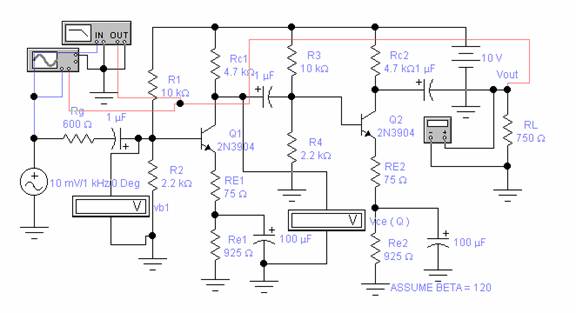
Figure 1 - Cascaded Common Emitter Swamped Amplifier (EWB Version 5)
VOLTAGE GAIN CALCULATIONS
For the amplifier circuit shown above, students will draw the dc
equivalent circuit and calculate the following DC quantities: VB,
VE, IE, VC, and VCE(Q).
Students will draw the ac
equivalent circuit and calculate the input impedance (Zin) for each
stage, and the unloaded voltage gain of each stage.
Students will determine the final output voltage (vout) by using the unloaded voltage gain and Thevenin's method or by using the loaded voltage gain method.
PRACTICAL LABORATORY CIRCUIT MEASUREMENT
In order to measure the ac voltage gain of the amplifier shown, students will first measure the dc voltages with no applied ac input voltage. If these are close to calculated values, then students will apply the ac input signal to the input of the amplifier, using a dual-trace oscilloscope to check the input and output signals. If the input signal is amplified, the DMM can be used to measure applied input, signal at base of each transistor, and final output voltage. Students should determine if the measured output signal (vout) is close to the calculated value? They should also determine if the output signal is in phase or out of phase with respect to the input signal?
TROUBLESHOOTING
Using a jumper wire and temporarily shorting the swamping resistor RE1, students will observe the effect on the output. After opening and shorting the 100 uF capacitor across Re1, students will record their observation of the output signal? Shorting the resistors, Rg, R2, Rc1, and RL one at a time, students will explain their observations of the output signal.
COMPUTER SIMULATION MEASUREMENT USING
ELECTRONIC WORKBENCH
(Version 5 or MultiSim version 2001)
Students will:
Load the Electronics Workbench and draw the amplifier circuit shown above.
Use the digital Multimeter (DMM) in DC mode to measure the DC voltages of VB, VE, VC, and VCE to determine if these values are close to calculated values.
Connect the sine wave source to the input of the amplifier and set the sine wave source for 10 mV (rms)/1kHz/0 Deg.
Attach the dual-trace oscilloscope to the input and output. (If they observe an amplified signal, their circuit is working and is ready for measurement.)
Measure the input signal at the base of each stage and the final output signal with an AC voltmeters and DMM as shown in the circuit shown above.
Use the bode plotter to measure the dB voltage gain
COMPUTER SIMULATION, DISPLAY OF RESULTS
The figure below shows the computer simulation of the laboratory experiment; the oscilloscope shows the input and amplified output signal. The bode plotter shows the measured dB gain of the amplifier.
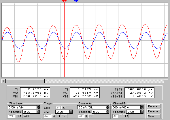
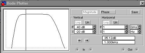
Figure 2 - Bode Plot dB Gain and Oscilloscope Display of Input & output Signal (EWB Version 5)
COMMENTS
Students will:
Compare their practical experiment, computer simulation, and
calculated values
Explain any significant differences between practical,
computer simulation, and calculated values.
Describe the function and purpose of each component in the
circuit.
Troubleshoot the cascaded CE amplifier and report their comments in a laboratory report.
REFERENCES
[1] Malvino, A. P., Electronic Principles, 5th edition, Prentice Hall: 1993 [2] Floyd, T. L., Electronic Devices, 3rd edition, Prentice Hall [3] Cox, J., Fundamental of Linear Electronics, Delmar [4] Boylstad, R. and Nashelsky, Electronic Devices, Prentice Hall [5] Mead, R. L., Foundations of Electronics, 2nd edition, Delmar: 1994 [6] Huffine, B., Common Emitter Amplifier Experiment, the Technology Interface: Spring 1997