|
|
Volume 4 No.1, Winter 2000 |
ISSN# 1523-9926 |
|
|
Volume 4 No.1, Winter 2000 |
ISSN# 1523-9926 |
|
Antonis K. Koukos |
ABSTRACT
This paper presents a connection identification system
and its hardware implementation architecture for use in ATM (Asynchronous
Transfer Mode) Networks. The system is responsible for connection recognition
and identification. This is applied to suitable connection identity fields.
These fields are VPI/VCI (virtual path/virtual channels identifiers). These
offered functions are useful for operation of terminals, switches, or
interworking units. The system has been implemented experimentally as part of
ATM network integrated circuits.
INTRODUCTION
Operation algorithm, design, and implementation
architecture of an ATM (Asynchronous Transfer Mode) Connection Identification
System (CIS) are presented in this paper. This
system is mainly used to support recognition and identification functions of
virtual paths/virtual channels (VP/VC)
in ATM Networks. The ATM method that has been standardized for use in IBCNs
(Integrated Broadband Communication Networks) use these channels whose value is
the connection identity. The flexibility in allocating bandwidth to connections
(VC) or groups of connections (VP) and the possibility to increase the
utilization of network resources through statistical multiplexing of bursty
traffic streams, are among the distinct advantages of the new information
transfer method. The system firstly extracts the connection identity fields, and
then, it searches to find if these fields belong to a used connection, or not.
In this way if the extracted VPI/VCI (Virtual Path/Virtual Channel Identifiers)
fields match with the stored ones then, the connection is used. This system
which can be used in terminals, in switches or, in interworking units implements
basic functions of the lower Layers of the ATM PRM (Protocol Reference Model)
[1], [2], [3], [4].
CONNECTION
IDENTIFICATION & OPERATIONAL ENVIRONMENT
CIS
is responsible for checking the VPI/VCI fields of cell headers. The role of it
is to inform other systems about the identity of cells. The received cells are
in parallel form (bytes) and transferred with a byte clock rate of 19.44 MHz
(~50 ns). Firstly, a unit extracts the VPI/VCI fields, provided that header
error control has done and the checked cell isn’t erroneous or has been
corrected. The fields are stored temporarily into a register until the begin of
a new time slot period. Then, the recognition/identification procedure begins
[5], [6]. According to this the extracted fields compared to other values of a
list. The list includes other used/unused VPI/VCI fields. If a matched field
found which corresponds to a used connection, then the current cell is accepted
and the operation control transferred to an other system. Otherwise, the current
cell doesn’t belong to a used connection.
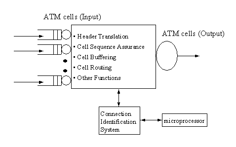
Figure 1(a). CIS in an ATM Switch
Figure
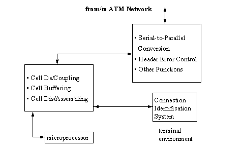
1(b). CIS in a Terminal
Environment
CIS can be used in a switch (Fig. 1(a)). It can support basic functions of the switch as header translation, cell routing and others are. In order to do these, connection identification must be done firstly. A microprocessor is responsible for the control of the system. CIS can be used in a terminal as well (Fig. 1(b)). It offers VPI/VCI fields recognition/identification when the cells are in microprocessor adapter of the terminal. In this way deactivated cells or idle cells can be discarded without being transferred to the terminal and so let it save cell transfer cycles. CIS can be used for recognition/identification of other types of cells as resource management, maintenance cells etc.
VPI/VCI
FIELDS RECOGNITION/IDENTIFICATION
Since
header error control operation has finished then, VPI/VCI fields are extracted
and stored with the rest of the header in a FIFO (First In First Out) system.
Extraction is done via suitable registers (24 bits) and appropriate logic gates,
which controlled by a Counter outputs. Since, VPI/VCI fields have been extracted
then, connection recognition/identification is done by a suitable system. It can
manipulate N different connections simultaneously. The accepted VPI/VCI values
(used connections or open connections) have already been stored into a table (VPI/VCI
Table), [7], [8]. These values consist of 24 bits according to CCITT
specifications [2]. Other 24-bit
values (masking bits) correspond to VPI/VCI values and enable or disable the
completely or partly use of VPI/VCI fields. Masking bits are stored into the VPI/VCI
Table as well (Fig. 2). The use of
these depends on the position of the Connection Identification system in the
network. The N VPI/VCI fields can be classified in s groups. Each group can be
assigned a 24-bit masking field and s may vary between 1 and N. The system
examines the values of VPI/VCI fields. It accepts cells that have VPI/VCI with
same value as stored VPI/VCI. Differently, the cell is rejected because
doesn’t belong to an active (open) connection. Every time slot when there is a
non-erroneous (or corrected) cell (Header_OK) with a new VPI/VCI identifier (VPI/VCI_avail=1)
(and the “bypass connection identity” procedure is disabled –
“NOTBypass_CI” logic is true) then, CIS examines the relation
(Header_OK)
AND (VPI/VCI_avail) AND (NOTBypass_CI)=1 (1)
If it is true then, table searching begins. A VPI/VCI Table Counter is used for producing the table addresses. The procedure has as follows (Fig. 3): When there is a VPI/VCI field in the table equal to the current cell VPI/VCI field (VPI/VCI_stored=VPI/VCI_extracted), then the signal “VPI/VCI OK” is activated (Comparison System). Then, the value of the masking bits is checked. If not all of them equal to “1” then searching stops and the current value of the table address (the contents of the VPI/VCI Table Counter) is provided (Connection_ ID) and is available to any system that needs the results of the connection recognition (e.g. a microprocessor). In this way the current cell is identified and translated. The “Connection_Valid” signal is activated. In systems as terminal receivers where a few connections can be open simultaneously a 4-bit table address is required. If the current VPI/VCI value doesn’t match to a table value of a current position then the system examines if the extracted VPI (only) field matches to a stored VPI field (VPI_stored=VPI_extracted). If yes, then the signal VPI_OK is activated. If not all of VPI Mask Bits equal to “1”, then the Connection_Valid signal is activated and the table searching is frozen. In all cases if all masking bits equal to “1” then searching is going on. Masking technique used as follows:
Every
bit
![]() (l=0...23) (VPI/VCI_Extracted) is
compared with every bit
(l=0...23) (VPI/VCI_Extracted) is
compared with every bit
![]() (VPI/VCI_Stored) in parallel. They
are used 24 masking bits
(VPI/VCI_Stored) in parallel. They
are used 24 masking bits
![]() (l=0...23) which value determines
if comparison cares. If it is true,
(l=0...23) which value determines
if comparison cares. If it is true,
![]() . If it isn’t true,
. If it isn’t true,
![]() . In this last case the extracted bit must be considered equal to the stored
bit. If it wouldn’t be considered equal and the rest-extracted bits were equal
to the rest stored bits, then the comparison resulted to an in-equation
(although the masked bits were “don’t care” bits). The system uses the set
of the logic equations:
. In this last case the extracted bit must be considered equal to the stored
bit. If it wouldn’t be considered equal and the rest-extracted bits were equal
to the rest stored bits, then the comparison resulted to an in-equation
(although the masked bits were “don’t care” bits). The system uses the set
of the logic equations:
xl
XOR x¢l
= cl ("l=0…23)
(2)
cl
AND (NOTx¢¢l)
= c¢l
("l=0…23)
(3)
In
the case that the compared VPI/VCI field is a “don’t care” pattern, then
all masking bits equal to 1 and
x¢¢0
AND x¢¢1
AND … AND x¢¢23
= 1 (4)
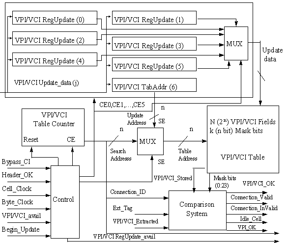
Figure
2.
VPI/VCI Recognition/Identification Circuit
Then,
the
![]() fed to a tree of OR gates. The
output gives the result of comparison. If the searching reaches the end of the
table (k=2n-1) without a valid connection found then, the searching
stops and the flag “Connection_Invalid”
takes the value “1”. For handling special cases, some positions have been
assigned special values. So, the first position (k=0) of the VPI/VCI table
includes the Idle Cell VPI/VCI field. When the extracted cell is idle the
matching with k=0 activates the flag Idle_Cell. Moreover, other types of cells
can be used as maintenance, metasignalling, unassigned cells etc. It must be
noticed that VPI/VCI table includes only used VPI/VCI fields. The remaining
positions (unused) of the table include the “Idle Cell” VPI/VCI field. In
addition, previously used connections continue to exist but they all have
masking bits equal to “1”.
fed to a tree of OR gates. The
output gives the result of comparison. If the searching reaches the end of the
table (k=2n-1) without a valid connection found then, the searching
stops and the flag “Connection_Invalid”
takes the value “1”. For handling special cases, some positions have been
assigned special values. So, the first position (k=0) of the VPI/VCI table
includes the Idle Cell VPI/VCI field. When the extracted cell is idle the
matching with k=0 activates the flag Idle_Cell. Moreover, other types of cells
can be used as maintenance, metasignalling, unassigned cells etc. It must be
noticed that VPI/VCI table includes only used VPI/VCI fields. The remaining
positions (unused) of the table include the “Idle Cell” VPI/VCI field. In
addition, previously used connections continue to exist but they all have
masking bits equal to “1”.
If
CIS must not be used, then a “bypass” procedure is used (Bypass_CI=1), then
the Connection_Valid flag takes the value of an external identification tag (Ext_Tag).
For
updating the stored values 7 registers are used. The first six (VPI/VCI
RegUpdate(0), VPI/VCI RegUpdate(1), VPI/VCI RegUpdate(5)) registers include the
new value of VPI/VCI that will be written to the table (masking bits are
included). VPI/VCI RegUpdate(6) includes the address value that shows the
internal table position that will be updated.
A flag shows if the registers are available for use (VPI/VCIRegUpdate_avail).
When writing ends (7 steps), then the CIS waits until the end of a current
connection identification searching that may occurs. Finally, the registers
contents transferred to the table.
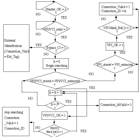
Figure
3. VPI/VCI
Recognition/Identification Algorithm
The
next figure (Figure 4) shows a snapshot of the implemented CIS functions. We can
see the exact timing of the system incoming data (RXHEADATA), incoming cells VPI/VCI
bytes (RXVPCI), mask bits (MASK), current cell validation signal (RXVPCIVALID),
selected VPI/VCI address signal SELVPCIADDR), incoming cell clock signal (RXCS),
current cell acceptance signal (ACCEPT) and other signals of the VPCI/VCI
Recognition/Identification system. The
circuit described in the previous, has been designed and implemented on an ASIC
chip using ECPD10 CMOS technology of the European Silicon Structure (ES2). The
VPI/VCI Table implemented for 16 connections and occupied silicon area of 0.63
mm2.
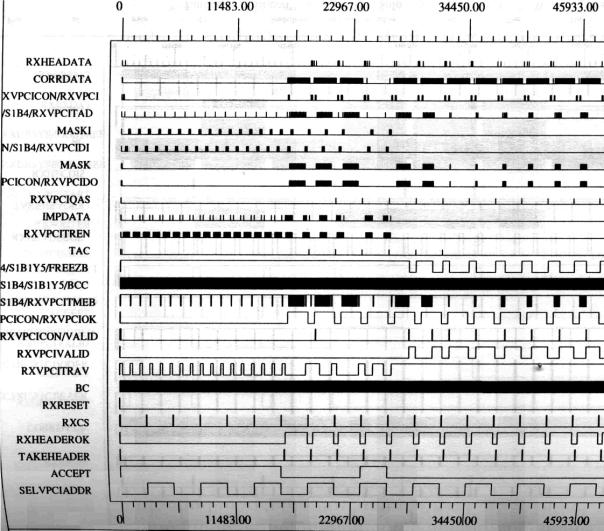
Figure
4. Implemented functions of
the VPI/VCI Recognition/Identification System
USE
OF CONTENT ADDRESSABLE MEMORIES-IMPLEMENTATION GUIDES
Content-Addressable
Memories (CAM) offers the possibility of applying associative processing [9].
They are useful to designs that require list searches and data translation as
embedded functions within systems. The combination of a CAM and a state machine
creates an economical controller [9], [10]. CAMs simplify the controller by
switching a lower-cost processor or a state machine. Associative processing
manipulates data based on matching, or associating an input value with other
values stored in an array. Associative processing hardware incorporates a
limited amount of computational capability at each memory location and allows
examining an entire memory array at once. In the previous system
(Fig. 2) the integration of a
memory (VPI/VCI Table), a counter (VPI/VCI Counter), a comparator (Comparison
System), some registers (VPI/VCI RegUpdate (j)), and glue logic constitute a CAM
system. The system has been
implemented in an ATM Receiver system circuit as a part of an ASIC chip [8],
[10]. The VPI/VCI Extraction part FIFO implemented with five registers in series
for saving area reasons. The VPI/VCI Recognition/Identification part uses a
table for storing VPI/VCI values. Using CMOS standard-cell technology (ES2 -
ECPD10 Process) ASICs were implemented by using megacell procedure. For
16-connections VPI/VCI fields (48 bits) a buffer of 1.68 mm2 silicon
is used. The design is synchronous and uses a 50 ns period clock (Byte Clock).
The implemented table operates using a 100 ns access time.
CONCLUDING REMARKS
In this paper design and circuit architecture of an ATM Connection Identification System are presented. This circuit, is mainly used to support connection identification functions for operation of terminals, switches or, interworking units. This is applied to suitable connection identity fields. It has been implemented experimentally as part of ATM network modules. The circuit can be very useful to everyone who develops ATM components and Networks
REFERENCES
Kawarasaki,
M. and Jabbari, B., “B-ISDN Architecture and Protocol,” IEEE JSAC, No 9, pp.
1405-1415, Dec. 1991.Vol. 9,
Minzer,
S.E., "Broadband and Asynchronous Transfer Mode (ATM)," IEEE
Communications Magazine,
p.p. 17-24, Sept. 1989
Black
Uyless: “ATM Foundation for Broadband Networks,” Volume 1, Prentice Hall,
Second Edition, 1999
Sato,
Y. and Sato, K., “Virtual Path and Link Capacity Design for ATM
Networks”, IEEE JSAC, Jan. 1991, Vol. 9, No 1 pp. 104-113.
Koukos,
A.K., Papadopoulos, A.I., Doumenis, G.A., Koukoutos, H.E., “The HEC BYTE
Generator-VCI Ectractor chip,” RACE Project 1022, NTUASWP4_1091PR_CC, Ver.
1.0, 6/14/92.
Koukos,
A.K., Kavidopoulos, K.A., Papaspyrides, A.C., Kamaras, J.G., Mitrou, N.M.,
“The ATM Receiver Integrated Circuit,” Hellenic
VLS.I Design and Prototyping
Environment,
HV/NTLC/0034, Ver. 1.2, 20/1/95.
Koukos,
A., Perissakis, S., “Communication Systems Development with the use of
ASICs,” in Proc. Technology
and Automation Conference, Piraeus, Greece, May,
9-10,1998
Weldson,
T., “Content-addressable memories add processing power to embedded
systems,” Electronic Design News, p.p 137-148, May 9, 1996.
Koukos, A., “(F)PGAs: A Technological Invitation-An Application: A PC Adapter for B-ISDN (ATM) Networks,”Panhellenic Association of Mechanical and Electrical Engineers Magazine, Nr. 273, p.p. 65-70, April 1995.