|
Novel Generations
of Inverting Current Conveyor Using Universal Current Conveyor
|
|
|
|
|
ABSTRACT
|
|
| Two novel types of current conveyor are introduced and defined in
this paper. Both types are from the family of inverting current conveyors.
They are the first- and the third- generation inverting current conveyors
(ICCI, ICCIII) in the concrete. A mathematical definition of their behavior and a method of their
realization are included. Their realizations are
done with help of Universal Current Conveyor (UCC) - novel versatile
circuit building block. The proposed UCC is a building block that
is able to replace any type of existing current conveyor. The CMOS design
of the universal current conveyor with reduced parasitic resistance on
the X-terminal is shown. PSpice simulations of the proposed circuits are
included. Finally, applications using these novel elements are presented. |
|
|
UNIVERSAL CURRENT CONVEYOR
|
|
Sedra and Smith introduced the first current conveyor in 1968. It was
called the first-generation current conveyor (CCI) [1] and it started the
evolution of this universal building block. Since then designers have developed
several variations of current conveyor. They have been called the second-generation
and the third-generation current conveyor (CCII, CCIII) [2, 3]. These building
blocks have found application in many fields, e.g. current-mode and mixed-mode
filter design, instrumentation and wideband amplifiers, and many more.
The most successful type is CCII. But, in some cases a disadvantage of
CCII can be observed. Conventional CCII cannot be used in applications
demanding differential or floating inputs like impedance converter circuits
and current-mode instrumentation amplifiers. Then the design of such an
amplifier requires two or more CCIIs. This problem has been solved with
the help of special current conveyors - current conveyors with differential
input (DDCC, DVCC) [4, 5].
The proposed universal current conveyor is a versatile building block
that is able to replace any type of existing current conveyor. In this
letter a detailed analysis of the proposed block is included inclusive
of small-signal analysis and basic PSpice simulations, which take into
account second-order effects. The design of UCC on the transistor level
using CMOS technology AMS 1.2mm is included
too. |
|
|
Definition and possibilities
|
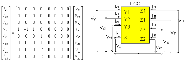
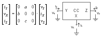
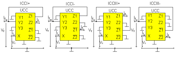
The universal current conveyor (UCC) is a novel eight-port building
block. UCC has three high-impedance inputs (differential Y1,Y2
and summing Y3 ), one low-impedance input X and
four current outputs (  ).
Outputs Z1, Z2 are complementary to outputs ).
Outputs Z1, Z2 are complementary to outputs  .
The matrix description of UCC and its symbol are shown in Fig. 1. .
The matrix description of UCC and its symbol are shown in Fig. 1.
|
|
Figure 1. Matrix description and symbol of UCC
|
The main advantage of the UCC is its versatility. All existing types
of current conveyor with single input could be realized with the help of
the UCC. This goal can be reached by using suitable connection between
terminals of the UCC. An example for CCI- is as follows:
CCI-
Y2, Y3 - grounded - vY2 , vY3 ,iY2
, iY3 missing
Y1, Z1 - connected - iY1=iZ1
vZ1, iZ1 missing
 , Z2- grounded
- , Z2- grounded
-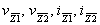 missing missing
 - output Z - output Z
Similar procedures realizing all the other types of current conveyor
can be found in Tab. 1 and Tab. 2. Moreover, a number of novel types of
current conveyor can be realized in this way. This will be demonstrated
in the following chapter.
|
|
|
Table 1. Realization of CC with single input
|
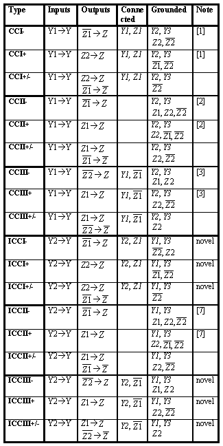
Table 2. Realizations of CC with differential input
|
|
Notice: Current conveyors, which are marked as "novel", haven't published
before.
|
|
UCC - CMOS implementation
|
| |
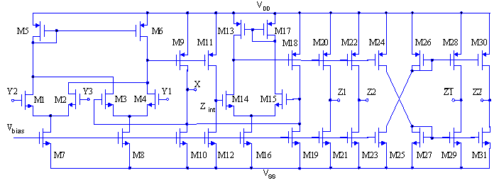
The first CMOS realization of UCC is shown in Fig. 2. All transistors
operate in saturation region. The input stage is similar to the DDCC
in [4].
|
|
Figure2. Basic CMOS implementation of UCC
|
The transconductance elements are realized with two differential stages
(M1 and M2, M3 and M4). Current mirror (M5 and M6) is a classical active
load, which provides a high-gain of the input stage. Moreover, it converts
the differential current to single-ended output current (M9), and then
the drain-currents equal |

|
| It is obvious |
|
| The output voltage in node X can be obtained as |
|
where A0 is the open-loop gain of amplifier (M1-M10) without
negative feedback from node X back to the amplifier (gate of M3)
and it is supposed that A0 is much larger than one.
One of the main advantages of this implementation is insensitivity
to the body effect. All the PMOS transistors have sources connected to
the positive supply rail. A similar situation exists in the case of NMOS
transistors. Their sources are connected to the negative supply rail, except
for M1-M4, which form differential pairs. But the error caused by body
effect is cancelled because the transistors in the differential pair have
the same source voltages and then the variations in threshold voltages
are the same.
|
| |
|
Figure 3. Block structure of UCC
|
|
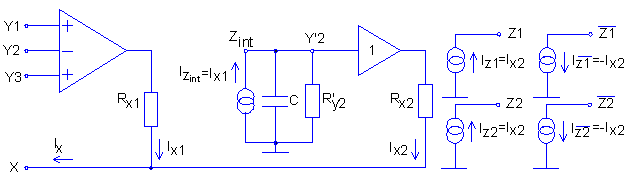
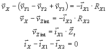
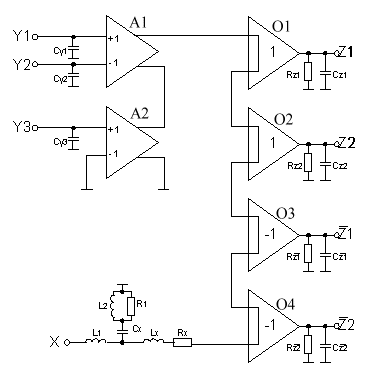
Transistors M13-M21 form an auxiliary current conveyor, which is connected
like a negative feedback to the current conveyor (M1-M12). This structure
is shown in Fig. 3 and described in [6]. The main goal of this connection
is lowering the parasitic resistance RX of the X-terminal.
The circuitry can be described by following equations |
|
where Zt is transfer impedance which is created by parallel
combination of R'y2 and C.
Now vx (when Y1, Y2 and Y3 are grounded) is can be
obtain as |
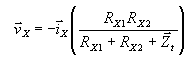
|
| and parasitic impedance can be obtained as |
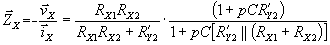
|
| where Rx1,2 is the parasitic resistance of appropriate
current conveyor and R'Y2 is input resistance of the
second current conveyor. The input resistance is close to Rx1Rx2/R'Y2
and it is very low (mW) due to R'Y2>>
Rx1,2. The circuit stability is ensured by compensation
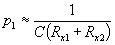
capacitor C. In proposed circuitry C is the parasitic capacitance
belong to CMOS structure and dominant pole p1 is then |
|
| Output terminal Z1 is formed by transistor M21 (it operates
like current source) and transistor M20, which duplicates the current of
transistor M18. Output Z2 is the same as output Z1 and they
form the positive types of current conveyor. Outputs
and operate
on the same principle, but their output currents have opposite direction
to Z1 and Z2. The small signal output resistance of the current
output terminals is determined by parallel connection of output resistances
of the transistors, which form each current output. Generally it is given
by |
|
where gdi, gdj are output conductance's of transistor Mi, Mj, respectively.
The biasing currents through transistors M7, M8 and M10, M12, M16,
M19, M21, M23, M25, M27, M29, M31 are equal to 150 mA
and 300 mA, respectively. |
|
|
Simulations and macromodel
|
|
Basic simulations of the UCC, which take into account the second-order
effects, are included in this section. Simulations were carried out by
standard PSpice circuit simulator. The described macromodel of UCC is based
on these simulations and was applied in the design of the following applications
using the UCC.
Model level which was used is level 2. Next rows show list of
some important parameters of used models:
nmos vth=0.736V,
cgso =0.290e-09 cgdo =0.290e-09 cgbo =0.170e-09
pmos vth=-0.751V
cgso =0.290e-09 cgdo =0.290e-09 cgbo =0.170e-09
The capacitances are per unit gate area.
The second order effects are effects like channel length modulation,
mobility degradation and bulk charge effects on current.
Figure 4. AC Voltage Transfer Vx/Vy |

Figure 5. AC Current Transfer Iz/Ix |
Figure 6. Parasitic Input Impedance Zx |
Figure 7. DC Current Transfer Izbar/Ix |
|
AC voltage transfer between Y- and X-terminal is shown in
Fig. 4. The input voltage was applied on Y1-terminal and its value
was 1 V. Other high-impedance input terminals and current-output terminals
were grounded. The cut-off frequency is 64 MHz.
Characteristics in Fig. 5 show ac current transfer from X- to
Z1-terminal.
High-impedance Y-terminals and Z2,,
-terminals were grounded. The cut-off frequency of the Z1-terminal
is 73.5 MHz. The value of applied input ac current was 100 mA.
Fig. 6 shows the parasitic impedance of the X-terminal and its dependence
on frequency. The value of frequency independent contribution of this impedance
(pure resistive contribution) is 4 mW. It can
be observe that the value of parasitic impedance on 1 MHz is still relatively
small (about 0.3 W). It can be achieved due
to described UCC structure.
The last characteristic in Fig. 7 shows the dc current transfer (from
X-terminal to -terminal).
High-impedance Y-terminals and Z1,Z2,
-terminals were grounded. The value of the applied current source (on X-terminal)
was changing from -250 mA to 250 mA.
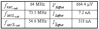
Important properties of the UCC, including voltage and current offsets,
are summarized in Tab. 3.
|
|
Table 3. Properties of the UCC
|
|
The previously simulation results are carried out by standard Pspice simulator.
The simulated file was a netlist file extracted from the schematic (Figure
2). The most accuracy simulations can be done with netlist extracted
from the layout of the proposed circuit (parasitic capacitances of MOS
transistors convergate more to real values).
Fig. 8 shows the macromodel of the UCC. It is composed of ideal current-followers
and differential voltage-followers. Parasitic elements model the frequency
behavior of a real UCC. The values of these components were derived from
the above PSpice simulations. This macromodel is simple but it is useful,
especially for simplified filter design using the UCC. The multifunction
filter included later in this paper was designed with the help of this
macromodel. |
|
|
Figure 8. Macromodel of the proposed UCC
|
|
|
NEW TYPES OF INVERTING CURRENT CONVEYORS
|
|
| The last current conveyor that was published is the second-generation
inverting current conveyor (ICCII) [7]. ICCII differs from CCII in the
negative voltage transfer between the Y- and the X-terminal. Next two missing
types of inverting current conveyor are introduced in this paper. A mathematical
definition of their behavior, the method of their realization with the
help of universal current conveyor (UCC) and applications using these novel
elements are presented. |
|
|
Definition of ICCI and ICCIII
|
|
Generally, a current conveyor (CC) is three-terminal device (except
special types of CC) and the relations between its ports can be described
by the matrix equation given in Fig. 9 with the general symbol of current
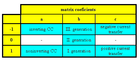
conveyor. Coefficients a, b, c determine each type of current conveyor
(coefficients can acquire values 0, -1 and 1).
|
|
Figure 9. Mathematical definition and symbol of general current
conveyor
|
|
|
|
Table 4. Definition of current conveyor with help of a, b, c
|
|
Concrete matrix description for each subtype of ICCI and ICCIII can be
derived from Tab. 4. The difference between CC and ICC of the same subtype
is only in the sign of voltage transfer between the Y- and the X-terminal. |
|
|
Realisations of ICCI and ICCIII
|
|
Novel types of inverting current conveyor, which were defined in the
previous chapter, have no special circuit implementation but they can be realized
with the help of universal current conveyor. This versatile building
block can replace all types of existing current conveyor with single input
including the novel types ICCI and ICCIII. UCC is a eight-port element
and the realization of each type of current conveyor can be obtained by
using a suitable connection between its terminals. Procedures realizing all the existing types of current conveyor can be found in Tab.1 and Tab.2.
The PSpice simulations of these novel conveyor exhibit resemblance to UCC
simulations. The UCC determines properties of the ICCI or ICCIII.
|
|
Figure 10. Realisation of ICCI and ICCIII with the help of UCC
|
|
|
|
Application based on ICCI and ICCIII
|
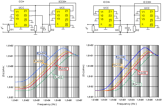
Synthetic grounded inductor (generally gyrator) is an application which
shows the usability of the novel types of inverting current conveyor. Two
possible realizations with the help of novel types of ICC are given in
Fig. 11. One realization consists of CCI+ and ICCIII+. The CCI+ is replaced
by ICCIII- in the other realization of gyrator. Both circuitries can be
described by the equation: |
|
|
|
Figure11. Synthetic inductor realizations and simulated results
(R1=R3=10 W, C=1 nF, R2 was a parameter)
|
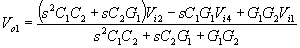
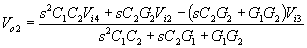
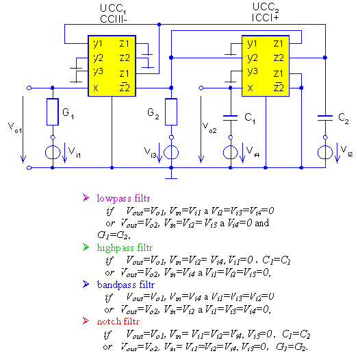
Another application using one of the novel types of ICC is the multifunction
network in Fig. 12. The input quantities are Vi1, Vi2,
Vi3
and Vi4 while the output quantities are Vo1
and Vo2. The complete circuit can be described by the
following equations:
For Vi3 = 0 we have |
|
| and if Vi1 = 0 then |
|
|
|
|
|
Figure 12. Multifunction network and possible filter
realizations
|
| It is evident from the above relations that the six-port can be applied
in the voltage mode (Vout/Vin) as filters,
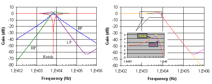
which are described in Fig. 12. The simulations in Fig. 13 show the transfer
characteristics of these filters (left-sided) and right-sided characteristics
compare response of lowpass filter with ideal UCC and real UCC. |
|
|
Figure 13. Simulations of multifunction network (C1 =C2=10
nF R1=1.7 kW, R2=2.9 kW,)
|
|
|
CONCLUSIONS
|
Two novel types of current conveyor, the first- and the second-generation
inverting current conveyor (ICCI and ICCIII), were presented in this paper.
Their behavior and circuit realizations with the help of universal current
conveyor were described. Applications which demonstrated the usage of the
novel elements were introduced. The application with ICCI was presented
in the case of multifunction six-port network, which realizes filter functions.
Simulations of these applications showed the practical usability of the
novel ICC. The novel ICCI and ICCIII can be inserted in the family of current
conveyors as novel and useful building blocks.
Next, a novel universal building block UCC was presented too. UCC is
able to replace all existing types of current conveyor with single input.
The versatility of the proposed block, which is the main advantage, was
demonstrated on the realizations of new types of inverting current conveyors
(ICCI and ICCIII). The UCC is useful as a generalization tool and design
concept for filtering applications and multifunctional circuits.
The versatility of UCC is paid by worse frequency behavior. Each special
designed current conveyor will be better from this point of view.
The future goal is the design and practical realization of UCC in BiCMOS
and bipolar technology, which will allow achieving more practical useful
values of the output currents, and realizing the UCC as universal device.
Then the practical usage of UCC as very universal discrete device will
be able.
|
|
ACKNOWLEDGEMENTS
|
This paper was carried out by project CEZ: J22/98: 262200011. |
|
|
REFERENCES
|
| [1] |
SEDRA, A., and SMITH, K.C.: "The current conveyor: A new circuit building
block", Proc. IEEE, Vol.56, pp. 1368-1369, Aug. 1968 |
| [2] |
SEDRA, A.S., and SMITH, K.C.: "A second generation current conveyor
and its application", IEEE Trans., 1970, CT-17, pp. 132-134 |
| [3] |
FABRE, A.: "Third-generation current conveyor: A new helpful active
element", Elec. Letters, Vol. 31, No.5, pp. 338-339, Mar. 1995 |
| [4] |
CHIU, W. and LIU, S.I.: "CMOS differential difference current conveyors
and their applications", IEE Proc.-Circuit Devices Syst., Vol. 143, No.2,
pp.91-96, 1996 |
| [5] |
ELWAN, H.O. and SOLIMAN, A.M.: "Novel CMOS differential voltage current
conveyor and its applications.", IEE Proc.-Circuits Devices Syst., 1997,
Vol. 144, No.3, pp. 195-200 |
| [6] |
PAYNE A. and TOUMAZOU C., "Practical integrated current conveyors.",
ISCAS'94 Tutorials, chap. 11.2.6, pp.595-596 |
| [7] |
AWAD, I.A. and SOLIMAN, A.M.: "Inverting second generation current
conveyors: the missing building blocks, CMOS realizations and applications",
Int.J.Electronics, 1999, Vol. 86, No.4, pp. 413-432 |
|
|
|