by
Bill Huffine
huffine@uscolo.edu
Department of Engineering Technology
University Of Southern Colorado
The Common Source Amplifier is one of the three basic FET transistor amplifier configurations. In comparison to the BJT common-emitter amplifier, the FET amplifier has a much higher input impedance, but a lower voltage gain. In this experiment, the student will build and investigate a simple n-channel, common source JFET amplifier. It is assumed that the student has had some background in basic transistor amplifier theory, including the use of simple ac equivalent circuits. The student is expec ted to develop his or her own procedure for performing the lab experiment, after having done a complete prelab analysis, and to then analyze, and thoughtfully summarize, the results of the experiment in a lab report. Additionally, the use of Electronics Workbench as computer simulation tool is described, to further enhance the learning process.
The purpose of this experiment is to investigate the operation of a common-source JFET transistor amplifier.
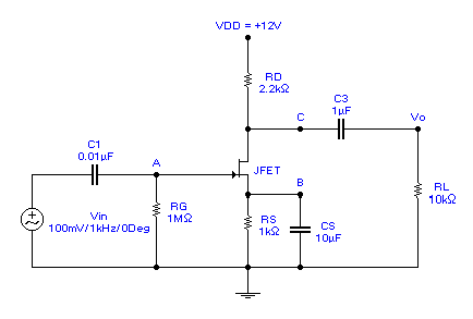
Some Circuit Notes:
1) The JFET is a general purpose, n-channel, JFET (2N5951, MPF102, or equivalent).
2) We will assume IDSS = 10 ma, VGS c/o = -4V, and gm = 2.5 mS in the prelab analysis.
Prelab
For the circuit shown, predict the following DC parameters: ID, VD, VG, VD, and VDS, using the "biasline technique". Recall that the operating point of the JFET can be found graphically from the intersection of the JFET "transconductance" or "transfer" equation (which relates ID to VGS) with the circuit biasline equation (VGS = - ID* RS). (A very rough approxi mation for this circuit is that VGS @ - 2V.)
Draw an ac equivalent circuit, and predict the voltage gain (Av), input impedance Zi, and output impedance Zo, assuming all capacitors act as "ac shorts". Also draw the "composite" waveforms expecte d at test points A, B, C, and Vo in the circuit, assuming the input signal Vin is a 100 mv peak, 1 kHz sinewave.
Also, draw a basic "black box" model (or equivalent circuit) for a voltage amplifier, consisting of an input impedance Zi, a dependent voltage source, and an output impedance Zo. (Recall that Zi appears across the input o f the amplifier, and Zo appears in series with the output of the amplifier's dependent voltage source). Refer to this simple equivalent circuit for the procedures that follow.You can measure Zi by inserting a test resistor (e.g: 1 Megohm) in series with the signal input to the amplifier, and measuring how much of the ac generator signal actually appears at the input of the amplifier (note the voltage divider betw een Rtest and Zi in your diagram). For example, if Rtest = Zi , the amplifier’s input signal will be half of the applied input signal. (N.B.: the input impedance of the test instrument may affect these readin gs!)
You can determine Zo as follows: temporarily remove the load resistor, and measure the unloaded ac output voltage. Then replace the load, and remeasure the ac output voltage. Use these measurements to determine Zo (note the voltage divider between Zo and RL in your equivalent circuit to help see this).
Lab Measurements
In-lab circuit measurements:
Build the circuit shown, and verify ALL of the predictions above. First check the DC quiescent voltages with no ac input signal. If these are reasonably close to your predictions, connect the ac input signal to the input of the amplifier. Use DC c oupling and dual-trace on the oscilloscope, as appropriate, to observe the waveforms at various points. Is the output signal (Vo) close to expected? How do the waveforms seen at the FET’s drain (point C) and the output (Vo) compare? What kind of wavef orm, if any, is seen at test point B? Then temporarily remove CS, and remeasure the output voltage; did it decrease as expected? Note that if you increase the input signal, Vo will increase, along with the non-linear distortion c reated by the variations in the FET transconductance, gm. You can reduce this non-linear distortion by adding a small "swamping resistor" of say 100 ohms at the source (explain how this works). What "price" is paid for thi s benefit?
Computer simulation using Electronics Workbench
Draw the circuit shown in Figure 1 using the editor within Electronics Workbench (EWB), except replace the terminal marked "VDD = +12V" with a +12V battery (to allow the simulator to work). Connect the amp lifier’s input to the sinewave signal generator in EWB. Use the DVM (digital voltmeter) in Electronics Workbench to measure the DC voltages at the FET terminals, and compare these to the predicted and measured values. Then connect the oscilloscope in EWB to various test points in the circuit, and compare these "measured" waveforms to your predicted and experimentally measured values.
Finally, try changing some of the circuit’s component values, and see how this affects the output signal; for example, by temporarily removing CS , you can see that the output signal dramatically decreases. By changing the source and drain resistors, it may be possible to further optimize the amplifier for a larger peak output signal. In summary, by using Electronics Workbench, note how easy it is to interactively change any component at will, and immediately see the effects, which further stimulates, encourages, and enhances the learning process.
For more accurate simulations in our case, we changed the ideal default JFET model in EWB to use the following JFET parameters, to more closely simulate the specified JFET with an IDSS of 10 ma and a VGS c/o of - 4V. For a JFET, a reasonably simple approximation for the drain current is that ID = Beta * (Vgs-Vto)2 , where Beta is the FET "transconductance coefficient", and Vto is the FET "threshold or cutoff voltage". We changed these parameters to: "Vto" = - 4V, and "Beta" = 0.00063 A/V2. (More information on these JFET parameters can be found in the Electronics Workbench and Pspice reference books, and in the last reference cited at the end of this a rticle.)
Comments and Conclusions
Compare your results with your prelab calculations. Explain any significant discrepancies. Also, explain clearly the purpose or function of the various components in the circuit; for example, what is the purpose of the source bypass capacitor? Why does a swamping resistor reduce the non-linear distortion, and at what cost? How does this circuit generally compare to a common-emitter amplifier?
Figure 1 - Common Source JFET Amplifier
Suggested References
"Common Emitter Amplifier Experiment including computer simulation", B. Huffine, Interactive Image Technologies, http://www.interactiv.com/html/huffine_article.html.
Electronic Devices, T. Floyd, Prentice Hall
Fundamentals of Linear Circuits, T. Floyd, Merrill
Electronic Devices and Circuit Theory, R. Boylestad and L. Nashelsky, Prentice Hall
Electronic Principles, A. Malvino, McGraw-Hill
Operational Amplifiers with Linear Integrated Circuits, W. Stanley, Prentice Hall
Reference Manuals for Electronics Workbench and Pspice
Spice: A Guide to Circuit Simulation And Analysis Using Pspice, P. Tuinenga, Prentice Hall
;