The application of the operational transconductance amplifier (OTA) in the design of simple amplifiers with voltage-controllable gain and to the design of firs-order and second-order active filters with controllable gains and controllable critical frequencies is demonstrated. A typical biasing scheme is also shown so that readers can more easily set up the circuits themselves.
This paper demonstrates the usefulness of the operational transconductance amplifier (OTA) as a replacement for the conventional op-amp in both first and second-order active filters. It is at least partially intended to acquaint the technology student w ith the rudiments of operation of the OTA, as well as the practicalities of using the presently available commercial OTA’s.
The structure of this paper is as follows. First, the basic operation of the OTA, including DC and AC operation, is explained. Simple example circuits will be presented in this section to demonstrate the similarities and differences between circuits w hich use the conventional op-amp and the OTA. Second, OTA active filter circuits will be presented and analyzed. The richness of the filter possibilities inherent in the second-order structures will be demonstrated. Finally, the last section will presen t practical considerations which must be considered when using the present generation of OTA’s.
1. DC Operation
The OTA is a transconductance type device, which means that the input voltage controls an output current by means of the device transconductance, labeled gm. This makes the OTA a voltage-controlled current source (VCCS), which is in contrast to the conventional op-amp, which is a voltage-controlled voltage source (VCVS). What is important and useful about the OTA’s transconductance parameter is that it is controlled by an external current, the amplifier bias current, IABC , so that one obtains
From this externally controlled transconductance, the output current as a function of the applied voltage difference between the two input pins, labeled v+ and v-, is given by
Clearly, an output voltage can be derived from this current by simply driving a resistive load. The equivalent circuit for the OTA is shown in Figure 1.
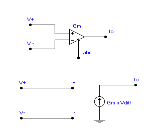 Fig. 1
At this point, two key differences between the OTA and the conventional op-amp must be kept in mind. First, since the OTA is a current source, the output impedance of the device is high, in contrast to the op-amp’s very low output impedance. Because a low output impedance is often a desirable trait in general amplifiers used to drive resistive loads, certain of the newer commercial OTA’s, such as National Semiconductor’s LM13600, have on-chip controlled impedance buffers. Second, it is possible to desi gn circuits using the OTA that do not employ negative feedback. In other words, instead of employing feedback to reduce the sensitivity of a circuit’s performance to device parameters, the transconductance is treated as a design parameter, much as resisto rs and capacitors are treated in op-amp based circuits.
The biasing of the OTA’s internal circuitry is such that the total quiescent supply current [Soclof-91] is given by ISUPPLY = 3IABC. This seems to imply that the OTA can be used in micropower applications, even down to IABC = 1 m A. However, the losses in speed and bandwidth, which are controlled ultimately by IABC, can be severe at such low current levels.
Much of the dependence of open- and closed-loop bandwidth and frequency responses in the OTA are similar to those in the conventional op-amp. For a circuit employing negative feedback, a very important relationship between the closed-loop bandwidth, the amplifier bias current, and the closed-loop gain exists:
where CNET is the sum of device junction capacitances at the output of the OTA and whatever load capacitance is attached to the circuit: CNET = CO + CL. Equation (3) has the interesting consequence that cer tain types of active networks, such as active filters, can have their critical frequencies controlled by the external current, IABC, which of course can be in turn controlled by an external voltage.
1. Basic Voltage Amplifiers
This section will discuss a subset of general voltage amplifiers, both with and without negative feedback. For further information about the rich variety of amplifier configurations available using the OTA, the reference [Geiger-85] is extremely useful.. Figure 2 displays an inverting amplifier realized with an OTA which can provide not only controllable gain, but which also uses negative feedback to reduce the output resistance. Indeed, the output resistance is also now controllable via the transconduct ance. The voltage gain and output impedance are given by
![]()
![]() (Eq. 5)
(Eq. 5)
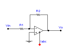 Fig. 2
The derivation of Equation (4) is presented in an appendix in order to demonstrate the typical analysis needed when dealing with OTA-based circuits. For the circuit in Figure 2, Equations (4) and (5) reduce to approximate forms for the case in which
![]() ; in this case, one obtains
; in this case, one obtains
Equation (6), of course, is nothing else than the in of a non-inverting amplifier. This is to be expected, since one of the properties of negative feedback is the nearly complete dependence of the gain on the feedback ratio only.
The final example of a basic building block amplifier using OTA’s is shown in Figure 3. This is an example of an all-OTA amplifier, with the voltage gain and output impedance given by
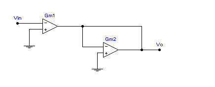
Fig. 3
The gain and output impedance are completely settable by the external currents, with no external, passive components except those needed to generate the current from a standard voltage source.
2. Active Filters with the OTA
Active filters are a standard application of the op-amp which can benefit greatly from the controllability of the OTA [Geiger-85]. The rudimentary theory and the circuit schematics for the basic active filters using op-amps are presented in many of th e textbooks in use in Electronics Technology or Engineering programs [Floyd-96 and Sedra-91]. What makes the OTA so attractive in these circuits is the ability to form filter circuits with voltage-variable control (via the IABC input) over a n umber of key performance parameters of the filter. The controlled parameter can be the midband gain of the circuit, as already realized in the simple circuits in the previous section. Alternatively, OTA-based active filters can use the external bias setti ng to control the location of the critical frequency, or 3-dB frequency, in a filter. The next logical step in controllability is the provision for independent gain and critical frequency setting. A number of other active filters can be realized with th e OTA. These provide the ability to not only change the critical frequency, the gain, or both, but also to preserve the shape of the response. For instance, one might want to control the critical frequency of the filter, but without altering the passban d ripple. It is even possible to change the type of response from lowpass to allpass to highpass by continuous adjustment of the transconductance gm. Only a very few of these alternatives can be developed in this paper.
A very simple example of a first-order (one pole corresponding to a roll-off rate of -20 dB/decade in frequency) lowpass filter is shown in Figure 4. The voltage gain over the whole frequency range , and the -3 dB frequency, is given by
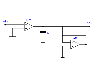
In this circuit the second OTA, labeled "Gm2", is configured as a voltage variable resistor. It is this variable resistor which provides the variable cut-off frequency in Equation (11).
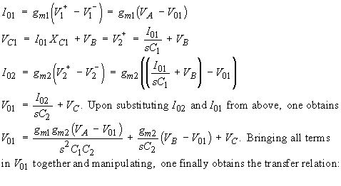
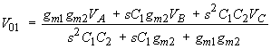
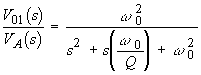
Figure 5 shows a second-order filter circuit with three voltage control terminals. Depending on which two of the three terminals are set to ground, one can realize a lowpass, highpass, bandpass, or notch filter. Each of these filters has a critical or center frequency which can be set by varying the transconductance, gm, of the two OTA’s in the circuit. These filters are called adjustable frequency constant-Q filters because they preserve the value of Q while the critical frequencies are s hifted. The derivation of the general relationship between the output voltage and the three control voltages is simply obtained:
 (Eq. 12)
 Fig. 5
In the above expressions, s is the complex frequency, s = jw , and I01 and I02 are the output currents for the first and second OTA’s, respectively.
An example of the reduction of Equation (12) to a specific filter type is provided by making the following settings:
The result is the following transfer function:
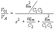 (Eq. 13)
This expression has the form of the standard biquadratic circuit [Sedra-91]:
 (Eq. 14)
Therefore, the circuit with these particular control voltage settings is a lowpass filter with a critical frequency given by :
and a constant  . It is straightforward to show that the following transfer functions can be obtained from the indicated control voltage settings:
3. Some Non-ideal Features of the OTA
One of the biggest drawbacks of the first versions [Harris-96, National-95] of the OTA was the limited range of the input differential voltage swing. This statement must be qualified in at least two ways. First, the limited input voltage swing appli es only if the OTA is being used in the open-loop configuration. In that case, if the difference-mode voltage exceeds about 25 mV, and the load resistance is relatively low (so that the open-loop gain is relatively small), then the circuit is no longer o perating in the linear region. This results in the output signal being distorted because of a nonlinear voltage transfer function [Sedra-91]. Of course, for circuits which make use of negative feedback, i.e., are operated in closed-loop conditions, then linear behavior is maintained.
The second qualifying remark is that the more recent versions of the OTA, such as the Harris CA3280A, National Semiconductor’s LM13600, and Philips’ NE5517, all use internal linearizing diodes at the input differential pair of the OTA. These make th e OTA’s output current a linear function of the amplifier bias current over a wide range of differential input voltages. Figure 6 displays a typical biasing scheme for a generic commercial OTA. The control voltage, VCTL, is used to generate t he amplifier bias current, IABC, through the resistor RABC. The linearizing diodes, which are incorporated on-chip in the commercial OTA’s mentioned above, can be biased on through the positive power supply voltage, +VCC. The analysis of the linearization circuit and its effect on the output current can be found in [Soclof-91] and in several of the application notes from the major vendors [National-95,Philips-94].
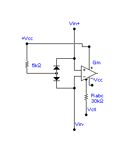 Fig. 6
IV. Conclusion
In conclusion, this paper has shown how the operational transconductance amplifier (OTA) adds controllability to a number of circuits commonly implemented with the conventional op-amp. In particular, an introduction has been given to the imp ortant class of voltage-controlled active filters realized with OTA’s. Sufficient introductory material of a tutorial nature has been included that the technology student and instructor can make use of the paper for further investigations.
Appendix
Template for calculating with OTA-based circuits
This appendix is meant to demonstrate, for students in particular, how one uses the ideal OTA equivalent circuit in order to predict the behavior of simple OTA-based circuits in the lab. Some of the approach will be suggestive of approaches taken t o the standard op-amp. In particular, the ideal OTA, just like the ideal op-amp, has a nearly infinite input resistance. This means that no current enters the OTA input pins, either inverting or non-inverting. However, the OTA is used often in open-loop, and therefore it is wise to learn how to treat the two input pins independently, as a virtual short circuit can not be assured in many configurations.
The circuit derivation that will be presented here is of the transfer function of, the inverting amplifier, Figure 2. The current IABC is presumed to be derived from a suitable biasing circuit. From the basic behavior of the OTA as a voltage controlled current source, one obtains
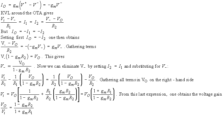
This completes the derivation of the voltage gain for this amplifier. Repeated application of these same assumptions and operations will yield the corresponding expressions for the other circuits discussed in the main body of the text.< /P>
References
Floyd, T., Electronic Devices: Conventional-Flow Version, 4th Edition, Chapter16. Prentice-Hall, Englewood Cliffs, N.J., 1996.
Geiger, R. L. and Sanchez-Sinencio, Edgar, "Active-Filter Design using Operational Transconductance Amplifiers: A Tutorial, " IEEE Circuits and Devices Magazine, Vol. 1, Number 2, pp. 20-32, March, 1985.
Harris Semiconductor, Application Notes 1174 (1996) and 6668 (1996), AN1174, AN6668.
Philips Semiconductor, Product Specification for NE 5517/5517A, "Dual operational transconductance amplifier", 8/31/94.
National Semiconductor, Application Note, "LM13600 Dual Operational Transconductance Amplifiers with Linearizing Diodes and Buffers", February, 1995.
Lenk, John D., Handbook of Practical Electronic Circuits, Chapter 10. Prentice-Hall, Inc., Englewood Cliffs, N.J., 1982.
Sanchez-Sinencio, E., Ramirez-Angulo, J., Linares-Barranco, B., and Rodriguez-Vazquez, A., "Operational Transconductance Amplifier-Based Nonlinear Function Syntheses," IEEE JSSC, Vol. 24, No. 6, pp. 1576-1586, Dec. 1989.
Sedra, A.S., and Smith, K.C., Microelectronic Circuits, 3rd Ed., Chapter 6. Saunders College Publishing, N.Y., 1991.
Soclof, Sidney, Design and Applications of Analog Integrated Circuits, Chapter 9.3. Prentice-Hall, Inc., Englewood Cliffs, N.J., 1991.