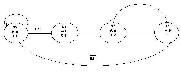
S0 = S0 * G0 + S3 * I < N
S1 = S0 * G0
S2 = S1 + S3 * I<N
S3 = S2
Accumulator Circuit
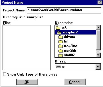
This contains the directory where the project will be stored (et398), and the name of the project (accumulator). Click the OK button. The system will inform you that the directory et 398 does not exist. Click YES to create it. Max+PLU SII will create the directory, and load this new project.
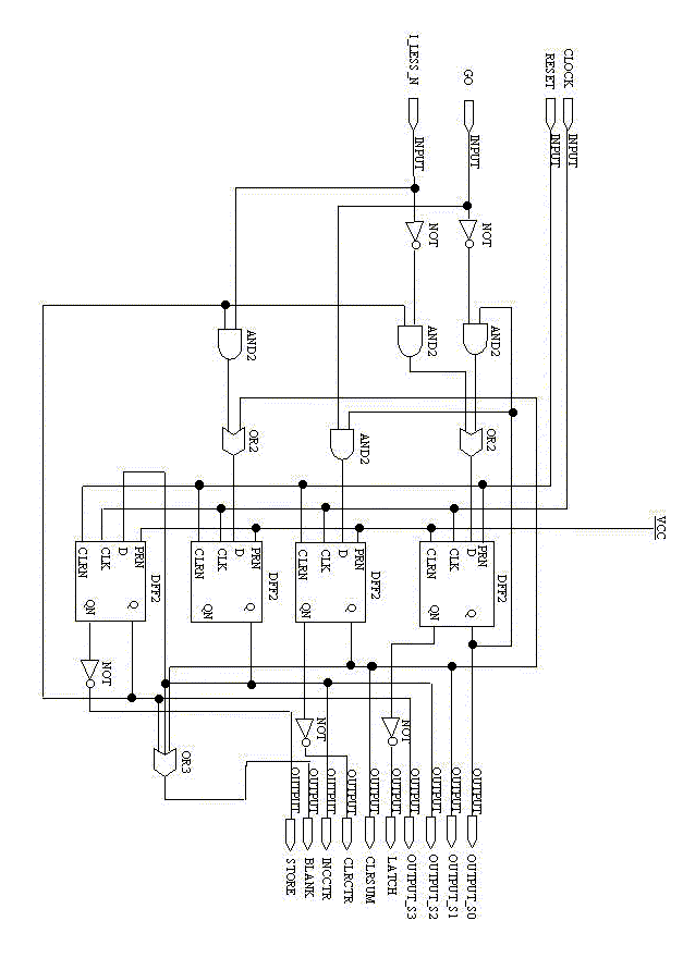
From your state equations S0 - S3, you can expect 4 Flip-Flops. Now you can start putting together your design.
9. Double click anywhere in the Graphic Editor window. A window
of libraries will pop-up.
10. Double click on c:maxplus2\max2lib\edif.
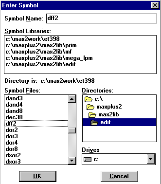
11. Clock on the ¯ in the Symbol Files: field to select dff2. (fig. 3)
A D Flip-Flop will appear on the Graphic Editor window. As you can see, it is very easy to scroll through Symbol Libraries to select the parts needed. Now, arrange the D Flip-Flop according to the schematic print out accumulator.gdf located in Appendix A. You can turn on the guidelines by clicking Show Guidelines from the Options menu. You can also set guidelines spacing from the options menu.
You will need 4 D Flip Flop, And-gates, 3 Or-gates, 5 inverters, 4 inputs, 1 VCC, and 10 outputs.
13. Double click anywhere in the Graphic Editor window.
14. Repeat steps 10 – 12 to get the second D-FF.
15. Double click anywhere in the Graphic Editor window.
16. This time just click OK.
17. Repeat steps 15 – 16 to get the last D-FF.
18. Double click anywhere in the Graphic Editor window.
19. Type or2 and click OK.
20. Repeat step 19 to get 1 more or2. 3 and2’s, 5 not’s, 1 or3,
and 1 VCC.
SHORTCUT: If more than one identical symbol is needed, hold down the <Crtl> key and the left mouse button on the symbol to be copied, then drag the mouse to a new destination, and let go the mouse. A copy of the symbol is made.
21. Arrange all of the parts (see Appendix A).
22. Enter 4 input pins by double clicking to the left of the screen. Type input and click OK.
23. Enter 10 input pins the same way: double click on screen, type output, click OK.
24. Name the input and output pins by double clicking on the default name "PIN_NAME". Be sure to type the names as on the schematic
provided (Appendix A).
NOTE: There are some characters that are reserved by the system and cannot be used as part of a name. Only letters, numbers, /, -, and _ can be used. So the "<" character cannot be used . Also, no spaces are allowed between characters.
SHORTCUT: Once you have aligned the inputs or outputs in a column, change the Name of the first one, then press <return> and it will take you to the Next pin. Do this until you have named all the Pins in a column.
It might be necessary to chose Line Style from the Options menu to select the solid line style. You can draw only straight lines or lines with a single bend this way. If you need to make more than one bend to connect a symbol, you will ne ed to release the line where you would like to turn, and pick it up again, dragging it to its destination.
26. Connect the rest of the lines as shown on the schematic
Appendix A.
27. After you finish, it is time to save the project. From the File menu, choose Project Save & Check. Make sure File Name is
"Accumulator.gdf" and that the Automatic extension is also .gdf
Click OK.
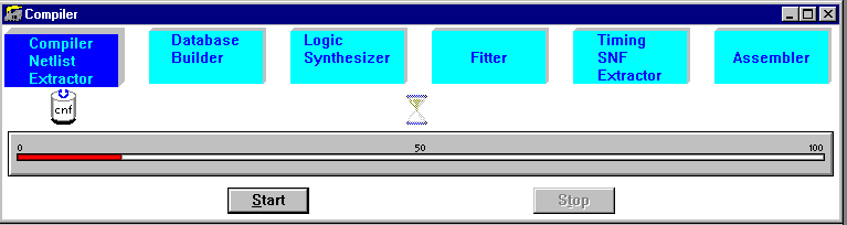
The compilation process starts, as shown in (fig. 4). If there are no errors or warnings, a windows will come up saying that Project Save & Check was successful. Click OK.
NOTE: If the window says Project Save & Check was unsuccessful, you did not follow instructions. Click OK and go to message-compiler window. Click on message and go to locate. The error area will be highlighted. If you cannot solve the problem , you can either use the content sensitive Help feature, or go to Help, Graphic Editor Help, Golden Rules. It is probably something minor. After fixing the problem, go back to step 27.
Now you need to finish the compilation. Hit the Start button.
The Message - Compiler window will come out. If there is only text in "Green" color, everything is fine. A window will come out saying: "Project Compilation was successful. Click OK. You can check your message now.
After checking your message, close Message - Compiler window and Compiler window.
28. From the file menu, choose Create Default Symbol.
This saves the file as a Symbol File (.sym), which will be used later on.
29. Choose Close from the File menu.
User-Defined Circuit
Now you will create a User-Defined circuit. NOTE: This part will only be used to demonstrate the use of the user-defined circuit.
1. Choose Project: Name, from File menu.
2. Type Myproject (or your name) in the Project Name box, making sure that c:\max2work\et398 appears as the current directory.
3. Choose OK. (The system load project: "Myproject").
4. Select New from the File menu.
5. From the File Type, select Graphic Editor file and .gdf file extension.
6. Choose OK.
7. Double click anywhere in the Graphic Editor window.
8. Double click on c:\max2work\et398 in the Symbol Libraries.
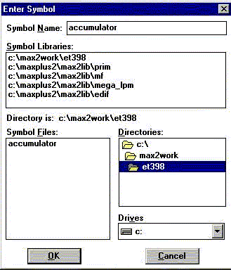
9. select accumulator from the Symbol Files (fig. 5)
10. Select OK.
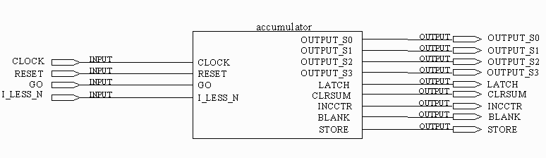
You will now see a chip that has the same inputs and outputs that you specified in your accumulator circuit. In fact, it is the same circuit. This can be verified by double-clicking on the symbol (fig. 6).
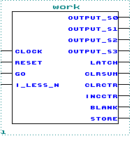
Fig. 6
11. Close the accumulator circuit from the File menu, to go back to
the user-defined circuit, myproject.
12. Get 4 input pins and 10 output pins, naming them as on
schematic Myproject (Appendix B).
13. Make all of the connections as shown on schematic Myproject (Appendix B).
14. Save & Check (Save as Myproject.gdf) and Choose OK.
15. Compilation process starts. If there are no errors, choose OK
from the Project Save & Check was successful window.
16. Compilation process needs to be finished. Press Start now.
17. Close Message - Compiler, and Compiler.
18. Close Myproject file from File menu. This time, it is not
necessary to create a symbol for this circuit, since it is
at the highest hierarchy.
If all of the previous steps have been followed correctly, you should now have a fully functioning accumulator. The next step is to simulate the project to see if it works as expected.
View Project Hierarchy
Before simulating the project, lets look at the Hierarchy Display.
1. Choose Hierarchy Display from the MAX+PLUSII menu (fig. 7).
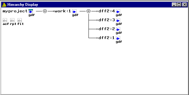
2. All files can be opened by double-clicking on them.
3. Close any open files.
4. Close Hierarchy Display.
Project Simulation
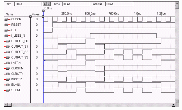
A comprehensive simulation follows, to test the performance of the project. The MAX+PLUSII Simulator is extremely easy to use and a very important step, not to be left out of the overall project creation. You can follow the accumulator simulation in Appendix B.
1. Choose New from the File menu.
2. Select Waveform Editor file and.scf file extension from the list.
3. Choose OK.
4. Go to File: End Time. Type an end tome of 1400ns and choose OK.
5. Go to Options: Grid Size. Type 50ns and choose OK.
6. Go to Node: Enter Nodes From SNF.
7. Under Type, turn off the All options, and turn on Inputs and
Outputs (fig. 8)
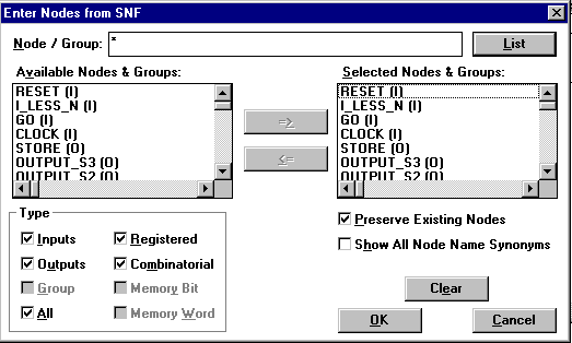
Entering Nodes from SNF.
8. Choose the List button to list available inputs and outputs.
After it simulates, you can go back and forth between waveform and simulation windows. When you first go to the waveform window, you might be looking at the end of the simulation, therefore, scroll the window back to the beginning, 0ns. When this is finished, you might want to experiment with the waveform to become familiar with its execution, by manipulating other input sections.
Programming Chip
1. Choose Compiler from the MAX+PLUSII menu.
2. Choose Device from the Assign menu.
3. Select MAX7000 from the Device Family (fig. 9).
4. Choose EPM7032DC-17 from Devices.
5. Click OK.
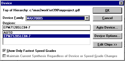
Selecting the programable logic device
6. From the Processing menu, choose Design Doctor Settings.
7. Select EPLD RULES: then OK.
8. Now choose Design Doctor from Processing menu.
9. Select Global Project Logical Synthesis from the Assign menu.
10. Select Normal from the Global Project Synthesis Style menu,
then OK.
11. Choose Timing SNF Extractor from the Processing menu.
12. Choose Report File from the Processing menu & select ALL.
13. Choose START from the Compiler menu.
If there are any errors or warnings, check to make sure that everything is typed in correctly or use the MAX+PLUSII content sensitive Help features.
14. Close the Compiler window.
Report File
The Report File contains information on: Device Summary, Project Compilation, File Hierarchy, Resource Usage, etc., as well as a pictorial pinout of the chip selected.
1. Choose Open from the File menu.
2. Select All Files.
3. Choose myproject.rpt
Review the whole document. You will find interesting information about your chip. It will tell you how to hook it up after you burn-it.
4. Close file.
Congratulations. You have finished this tutorial. The next step is to put your design on a Hardware device.