The article shows in detail how to use operational transconductance amplifiers (OTA) to design basic sinusoidal oscillators based on the active-filter tuned oscillator topology. The specific contribution that the OTA makes to the oscillator design is the ability to achieve voltage control of the center frequency and Q of the active filter from the tunable transconductance of the OTA. This in turn gives the user control over the oscillation frequency.
The aim of this paper is to show the design and synthesis of a voltage-controlled oscillator(VCO) using the operational transconductance amplifier(OTA) as the active element in place of the conventional op-amp. The voltage control tech nique will be applied to a second-order bandpass filter. The bandpass filter is part of an overall feedback loop with a hard limiter circuit. This type of scillator is called an active-filter tuned oscillator[1]. The voltage control made possible by th e use of the OTA enables the designer to synthesize oscillators with adjustable frequencies of oscillation. At the same time, the OTA-based active filter can be adjusted not only for center frequency, but also for filter Q or bandwidth. One would adjust filter Q as the filter's center frequency is adjusted in order to maintain a constant bandwidth. The maintenance of constant bandwidth while the center frequency is changed ensures that the oscillator's output waveform has the desired purity. This pape r will demonstrate how the OTA can serve as the active element in voltage-controllable filters and oscillators.
The structure of this paper is as follows. First, a review of the concept of the active-filter-tuned oscillator will be presented. Second, a specific second-order voltage-controlled bandpass filter implemented with the OTA will be disc ussed. This particular choice is made because of its ability to control both center frequency and Q via external control signals. Finally, the design of the OTA-based voltage-controlled oscillator will be presented.
In this section, the basic principles of operation of the active-filter-tuned oscillator will be presented [1]. Once the principle of this oscillator topology is understood, the ease of incorporating the OTA in the bandpass filter loop
of the oscillator will be apparent. Figure 1 shows a block diagram schematic of the oscillator. The oscillator operates in the following manner. Assuming that oscillations have started, the output of the bandpass filter will be a sine wave with a fr
equency equal to the center frequency of the filter. This sine wave, ![]() , is fed back into a hard limiter, which can be realized with a conventional op-amp. The limiter produces as its out put a square wave, V1
, with a fundamental frequency equal to the frequency of the sine wave. The square wave amplitude is set by the saturation limits of the limiting circuit. The square wave in turn is fed back into the bandpass filter, which filters out harmonics to
produce a sinusoidal output. The key to the successful generation of a high-purity sine wave is the selectivity of the filter, or the Q value. In the OTA-based oscillator proposed in this paper, not only will the center frequency of the filter be adjusta
ble, but the Q as well. The advantages of the active-filter tuned oscillator are the independent control of frequency and amplitude, the control of the distortion in the output sinusoid, and the fact that any bandpass filter circuit with a positive gai
n can be used. The use of the OTA as a replacement for the conventional op-amp in the bandpass filter portion of the circuit enhances these advantages by providing the circuit with independent voltage control of the frequency and the selectivity of the fi
lter.
, is fed back into a hard limiter, which can be realized with a conventional op-amp. The limiter produces as its out put a square wave, V1
, with a fundamental frequency equal to the frequency of the sine wave. The square wave amplitude is set by the saturation limits of the limiting circuit. The square wave in turn is fed back into the bandpass filter, which filters out harmonics to
produce a sinusoidal output. The key to the successful generation of a high-purity sine wave is the selectivity of the filter, or the Q value. In the OTA-based oscillator proposed in this paper, not only will the center frequency of the filter be adjusta
ble, but the Q as well. The advantages of the active-filter tuned oscillator are the independent control of frequency and amplitude, the control of the distortion in the output sinusoid, and the fact that any bandpass filter circuit with a positive gai
n can be used. The use of the OTA as a replacement for the conventional op-amp in the bandpass filter portion of the circuit enhances these advantages by providing the circuit with independent voltage control of the frequency and the selectivity of the fi
lter.
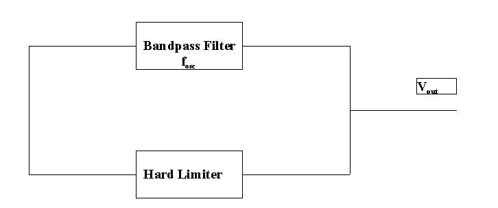
Figure 1. Active-filter tuned oscillator: block diagram
The following section will describe the operation of an OTA-based active filter. This filter provides the designer with the ability to control independently both the center frequency and the Q of the filter. It is this independent cont rol which is most important for the active-filter-tuned oscillator.
III. OTA Active Filters
The basic operation of the operational transconductance amplifier (OTA) is reviewed in a number of texts and articles on a variety of levels [2-5]. The article by Geiger and Sanchez-Sinencio [5] is a valuable account of OTA-based ampli
fiers and filters. Figure 2 shows the basic schematic and equivalent circuit for the OTA [6]. The OTA is a transconductance type device, which means that the input voltage controls an output current by means of the device transconductance, labeled ![]() . This makes the OTA a voltage-controlled current source (VCCS), which is in contrast to the conventional op-amp, which is a voltage-controlled voltage source (VCVS). What is important and useful about the OTA’s tran
sconductance parameter is that it is controlled by an external current. This external current is called the amplifier bias current,
. This makes the OTA a voltage-controlled current source (VCCS), which is in contrast to the conventional op-amp, which is a voltage-controlled voltage source (VCVS). What is important and useful about the OTA’s tran
sconductance parameter is that it is controlled by an external current. This external current is called the amplifier bias current, ![]() , so that one obtains
, so that one obtains
| (Eqn. 1) |
From this externally controlled transconductance, the output current as a function of the applied voltage difference between the two input pins, labeled ![]() is given by
is given by
| (Eqn. 2) |
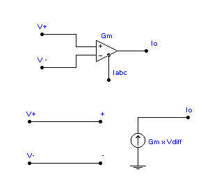
Figure 2. Equivalent circuit of OTA
Figure 3 shows a second-order filter circuit with three voltage control terminals. Depending on which two of the three terminals are set to ground, one can realize a lowpass, highpass, bandpass, or notch filter. Each of these filters ha
s a critical or center frequency which can be set by varying the transconductance, ![]() , of the three OTA’s in the circuit. These filters are called adjustable frequency adjustable-Q filters because the center freque
ncy and the Q are independently controllable. Because of this independent control, it is possible to realize a constant bandwidth over a wide range of center frequencies.
, of the three OTA’s in the circuit. These filters are called adjustable frequency adjustable-Q filters because the center freque
ncy and the Q are independently controllable. Because of this independent control, it is possible to realize a constant bandwidth over a wide range of center frequencies.

The derivation of the general relationship between the output voltage and the three control voltages is simply obtained:
![]()
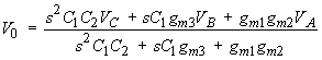 | (Eqn. 3) |
In the above expressions, s is the complex frequency, ![]() and
and ![]() are the output currents for the OTA’s. One can synthesize a bandpass filter from the tra
nsfer function in Eq. (3) by setting
are the output currents for the OTA’s. One can synthesize a bandpass filter from the tra
nsfer function in Eq. (3) by setting ![]() to ground and
to ground and ![]() to the input voltage. The transfer function then becomes:
to the input voltage. The transfer function then becomes:
| (Eqn. 4) |
It is possible to transform this expression into one which will instantly yield the value of the center frequency and Q (and thus the bandwidth). In the particular case of Eqn. (4), dividing both numerator and denominator by the prod
uct ![]() gives the following:
gives the following:
 | (Eqn. 5) |
This transfer function is of the form
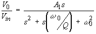 | (Eqn. 6) |
This is the standard form for a second-order bandpass filter [1]. Therefore, the center frequency of this filter is
 | (Eqn. 7) |
while the -3 dB bandwidth is found directly from the transfer function to be
| (Eqn. 8a) |
| (Eqn. 8b) |
Because this circuit is to be called on to form the feedforward loop of an oscillator, it will be important to understand the relationship between the bandpass center frequency and the filter Q. The result for the Q of the circuit is< /P>
 | (Eqn. 9) |
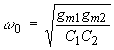
By setting ![]() , it is clear from Eqn. (7) that the center frequency can be made linearly dependent on
, it is clear from Eqn. (7) that the center frequency can be made linearly dependent on ![]() :
:
| (Eqn. 10) |
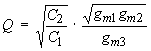
At the same time, ![]() can be separately adjusted to yield a controllable value for the filter Q:
can be separately adjusted to yield a controllable value for the filter Q:
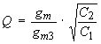 | (Eqn. 11) |
Therefore, the bandpass filter realized in this fashion has independently controllable center frequency and Q. This control comes about through the control over the transconductances of the OTA’s in the filter circuit. The transconduct ance are determined by the external bias current, or what is called the amplifier bias current, IABC (see Eqn.1). As shown in Figure 5, the amplifier bias current can be controlled via an external voltage, labeled Vctl in the figure, applied a cross a biasing resistor, labeled Rabc in the figure. Finally, because of the independant control over the bandpass filter center frequency and Q, the bandwidth can be maintained at a constant value. Keeping a constant bandwidth as center frequency is a djusted is important for the overall quality of the sinusoidal waveform generated in the active-filter-tuned oscillator.
In this section, the design of an active-filter tuned oscillator based on the OTA will be presented. Figure 4a shows a simple realization, using a conventional op-amp and two Zener diodes, of a bounded comparator used as a hard limiter. With the limiting circuit displayed here [1], the transfer curve has the following saturation voltages
| (Eqn. 12a) |
| (Eqn. 12b) |
where ![]()
Figure 4b shows the complete oscillator circuit, including the OTA-based bandpass filter. Several points should be made about this circuit. In the first place, the most recent commercial OTA’s, National Semiconductor’s LM13600 [7], Phil ips Semiconductor’s NE5517 [8], and Harris Semiconductor’s CA3280 [9], all have linearizing diode circuits at the input to the OTA. These linearizing diodes are necessary in order to increase the range of input differential voltages that will maintain th e OTA in its linear region of operation. Secondly, the LM13600 and the NE5517 now provide the user with controlled impedance buffers, so that a low output impedance might be used when interconnecting amplifiers. Figure 5 displays a fuller version of an O TA such as the LM13600 which shows the linearizing diode bias connection, the external control voltage used to generate the amplifier bias current, and the output buffer transistors used to provide low output impedance. The connections shown in Figure 5 are all internal to the OTA, except for the Vctl-Rabc biasing connection. The circuits displayed in Figures 1-3 and Figure 4c are to be understood as including the necessary control voltages for the amplifier bias current, IABC, the linearizin g diode, ID, and the power supply connections.
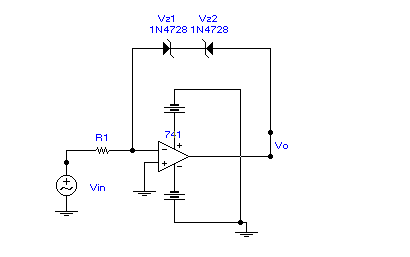
Figure 4a. Simple limiter circuit
Thirdly, the user or circuit designer must be aware that the OTA, which can be used with or without negative feedback, will necessarily have limitations on the magnitude of the input differential voltage swing. For instance, the LM136
00 [7] has an absolute maximum rating of ±5 Volts for the input differential voltage. On inspecting the circuit Figure 4b, one sees that OTA-1 has its positive signal pin tied to ground, while its negative signal pin is connected directly to the outp
ut voltage. Therefore, without exercising caution in the signal design for this circuit, it is possible for OTA-1 to see a dangerously high differential input voltage. It is also clear that ![]() is equal to the mag
nitude of the saturation voltages in Eq. (12), so that the output voltage magnitude of the oscillator at the center frequency will be:
is equal to the mag
nitude of the saturation voltages in Eq. (12), so that the output voltage magnitude of the oscillator at the center frequency will be:
| (Eqn. 13) |
If, as an example, the Zener diodes are 1N4728 types, they will have a Zener voltage of about 3.3 Volts, giving a ![]() Volts. If, in order to have a margin of safety on the maximum differential in
put voltages, one decides to tolerate ±
4 Volts, then the usefulness of the constant gain bandpass filter becomes clear.
Volts. If, in order to have a margin of safety on the maximum differential in
put voltages, one decides to tolerate ±
4 Volts, then the usefulness of the constant gain bandpass filter becomes clear.
Finally, it is important to understand in an intuitive way why the filter’s Q needs to be settable. Basically, as the center frequency of the bandpass filter varies over a wide range, it is desirable to keep the bandwidth nearly co nstant. A constant, narrow, bandwidth is needed to generate a reasonably pure sine-wave by filtering the square wave that the bounded comparator has produced. The square wave from the comparator has many sine-wave components in its spectrum i.e., the fu ndalmental frequency and odd harmonics of that frequency in ever-decreasing amplitude. it is essential that the bandpass filter have a sufficiently narrow bandwidth so that the small, high frequency ripples due to these higher harmonics do not appear in the output sine wave.
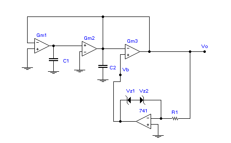
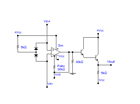
Figure 5. Biasing scheme for OTA, including output buffer
This paper has presented a new design for a voltage controlled active-filter tuned oscillator in which the controllability is implemented by the use of operational transconductance amplifiers (OTA). Significant detail has b een given that should enable instructors and others to construct the circuit. Finally, sufficient analytic detail has been provided so that well-motivated students can analyze any of the many other circuits which use OTA’s as their active elements. < /P>
References
1. Sedra, A.S., and Smith, K.C., Microelectronic Circuits, 3rd Ed., Chapter 11. Saunders College Publishing, N.Y., 1991.
2. Floyd, T., Electronic Devices: Conventional-Flow Version, 4th Edition, Chapter 16. Prentice-Hall, Englewood Cliffs, N.J., 1996.
3. Soclof, Sidney, Design and Applications of Analog Integrated Circuits, Chapter 9.3. Prentice-Hall, Inc., Englewood Cliffs, N.J., 1991.
4. Lenk, John D., Handbook of Practical Electronic Circuits, Chapter 10. Prentice-Hall, Inc., Englewood Cliffs, N.J., 1982.
5. Geiger, R. L. and Sanchez-Sinencio, Edgar, "Active-Filter Design using Operational Transconductance Amplifiers: A Tutorial, " IEEE Circuits and Devices Magazine, Vol. 1, Number 2, pp. 20-32, March, 1985.
6. Grise, W. R., "Application of the Operational Transconductance Amplifier (OTA) to Voltage-controlled Amplifiers and Active Filters", TECHNOLOGY INTERFACE: The Electronic Journal for Engineering Technology, Vol. 2, # 2, Winter ‘98. URL: http://et.nmsu.edu/~etti
7. National Semiconductor, Application Note, "LM13600 Dual Operational Transconductance Amplifiers with Linearizing Diodes and Buffers", February, 1995.
8. Philips Semiconductor, Product Specification for NE 5517/5517A, "Dual operational transconductance amplifier", 8/31/94.
9. Harris Semiconductor, Application Notes 1174 (1996) and 6668 (1996), AN1174, AN6668.