|
|
Volume 4 No.1, Winter 2000 |
ISSN# 1523-9926 |
|
|
Volume 4 No.1, Winter 2000 |
ISSN# 1523-9926 |
| Ahmad
Zargari, Ph.D., CSIT Associate Professor a.zargar@morehead-st.edu http://people.morehead-st.edu/fs/a.zargar/ Morehead State University Morehead, Kentucky |
Michael
S. Combs, MS Senior Technician Morehead State University Morehead, Kentucky |
ABSTRACT
In today’s industry and research laboratories more applications are calling for control and data acquisition (DAQ) devices. Personal computers have become a primary tool in data acquisition with the development of hardware and software interfaces. Interface packages used in industry can be expensive in the educational lab setting more cost-effective interface cards may be built to demonstrate the theory and operation of these devices. Building the interface card gives the student much more than just teaching the operation of the device. Students learn the design and inter workings of the interface card. Several different skills are needed and acquired throughout this project, and with the demand if interfacing in industry it proves to be a needed educational tool.
The project consists of building an interface card, which is inserted into a PC ISA slot. The card utilizes an 8255 programmable peripheral interface IC that has up to 24 digital I/O lines. Circuit design, board layout, test circuit, and software routines are discussed.
INTRODCUTION
The network adapter card or network interface card (NIC) plugs into the computer's bus, and a cable connects it to the network medium (Comer, 1999). The interface card is essentially a digital input/output device used to interface a personal computer with the outside world. A personal computer is a powerful tool and has an infinite amount of capabilities and applications. The interface card extends these capabilities to the outside world. The board can be used for both controlling and monitoring processes through software routines and sensors. The only limitation is the user’s imagination.
The interface card is inserted into the personal computer’s bus through an ISA slot. A connector is attached to the board to allow it to connect with the outside world. Here devices, which need to be controlled, are attached, along with the sensors needed to monitor the device or process.
With the mixture of the interface card, software routines, and support electronics a powerful tool can be developed.
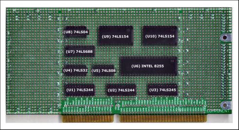
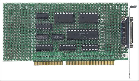
ISA PROTOTYPE BOARD
Prototype boards have been designed to be plugged directly into various PC bus slots (Triebel, 1998). This interface card uses a prototype board designed for the ISA bus architecture. This bus architecture is common in today’s PCs. The prototype board is the base for which all circuitry will be placed. Figure 1 displays the ISA prototype board used in this project.
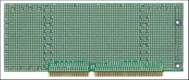
Figure 1. ISA Prototype Board
The interface card has a total of ten ICs and various parts. Table 1 illustrates the parts list followed by descriptions of the parts for the interface card. This list does not include the support circuitry needed for testing the board.
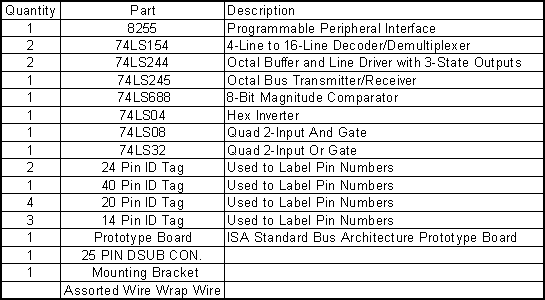
Table 1. Parts list
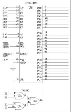
Figure 2 illustrates the pinout of 8255 Programmable Peripheral Interface (PPI).
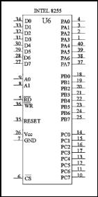
Figure 2. The pinout of the 8255 A
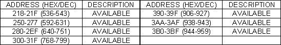
The IC used for interfacing is the 8255 PPI. This chip is designed and manufactured by Intel. The 8255 Interface Adapter is a programmable peripheral interface device designed for use in microcomputer interfacing systems. It is a general purpose I/O device that can interface any TTL compatible peripheral device to a microcomputer system. The 8255 has 24 pins of I/O, programmable and configurable by software, in two groups of 12 pins, that are used in three separate modes of operation (Brey, 1995). The Interface Adapter is selected by its CS line for programming and for reading and writing to a port. Port assignment and register selection is accomplished through the A1 and A0 pins. Table 2 shows the I/O port assignments used programming and access the I/O ports (Rafiquzzaman, 1995; Uffenbeck, 1998).
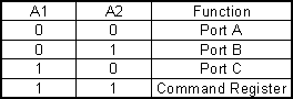
Table 2. I/O port assignments
For the 8255 to be read from or written to, the CS line must be a logic low and a correct I/O address must be applied to the A0 and A1 pins. The Read/Write and Control Logic block is used to manage all of the internal and external transfers of both Data and Control or Status words. It accepts inputs from the CPU Address and Control busses and in turn, sends commands to the Control Groups of the 8255. Each 8255 port is programmed through system software to determine its function. This is done when the CPU “outputs” a control word to the 8255. The control word initializes the functional configuration of the 8255. Information such as "mode", "bit set", "bit reset", etc., is contained in the control word.The
command byte of the command register selects either command byte A or command
byte B. If bit 7 of the command is
0, command byte A is selected. If
bit 7 of the command register is 1, command byte B is selected.
Command byte A programs the function of group A and group B.
Command byte B sets or rests bits of port C only if 8255 is programmed in
mode 1 or 2 (Brey, 1995). Each of
the control groups (Group A and Group B) accepts "commands" from the
Read/Write Control Logic block, and also receives "control words" from
the internal data bus and issues the proper commands to its associated ports.
Control Group A consists of Port A and upper part of Port (C7-C4). Control Group
B consists of Port B and Port C lower part (C3-C0).
The 8255 contains three 8-bit ports (A, B. and C). All can be configured
in a wide variety of functional characteristics by the system software but each
has its own special features or "personality" to further enhance the
power and flexibility of the 8255.
Port
A.
One 8-bit data input/output latch/buffer. Both "pull-up" and
"pull-down" bus hold devices are present on Port A.
Port B.
One 8-bit data input/output latch/buffer. Only "pull-up" bus hold
devices are present on Port B.
Port C.
One 8-bit data output latch/buffer and one 8-bit data input buffer (no latch for
input). This port can be divided into two 4-bit ports under the mode control.
Each 4-bit port contains a 4-bit latch and it can be used for the control signal
outputs and status signal inputs in conjunction with ports A and B. Only
"pull-up" bus hold devices are present on Port C.
The 8255 PPI has
three modes of operation (Modes 0, 1, 2), which designate the function of each
port (Subbarao, 1992; Triebel & Singh, 1997). In Mode 0,
Ports A and B operate as either inputs or outputs and Port C is divided into two
4-bit groups either of which can operate as input or output. Mode 1 operation is
the same as Mode 0 but Port C is used for handshaking and control. In Mode 2,
Port A is bi-directional (both input and output) and Port C is used for
handshaking, but Port B is not used. This IC allows the interface card to have
flexibility. The Modes are selected by software commands in the programs written
for the card. Table 3 shows the
control words and their associated settings for the different modes of
operation.
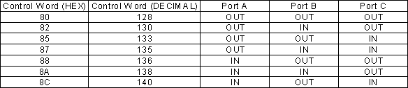
Table 3. Control words and their settings
74LS154 4-LINE 16-LINE DECODER/DEMULTIPLEXER
The 74LS154 is a 4-line to 16-line decoder/demultiplexer. The 74LS154 decodes four binary-coded inputs into one of sixteen mutually exclusive outputs. In order to enable the IC both the strobe inputs, G1 and G2, are set low. Demultiplexing is accomplished by using the 4 input lines to address the output line. All outputs are high when either strobe input is high.
74LS244 OCTAL BUFFER AND LINE DRIVER
The 74LS244 is an octal buffer and line driver with 3-state outputs. The 74LS244 is designed to be used as, clock drivers, memory address drivers, and bus-oriented transmitters/receivers.
74LS245 OCTAL BUS TRANSMITTER/RECEIVER
The 74LS245 is an octal bus transmitter/receiver designed for 2-way asynchronous 8-line data communication between data buses. The DIR pin controls data direction from bus A to bus B or bus B to bus A depending upon its logic level. The Enable pin can be used to isolate the buses.
74LS688 8-BIT MAGNITUDE COMPARATOR
The 74LS688 is an 8-bit magnitude comparator, which performs comparisons between two eight-bit binary or BCD words.
LOGIC GATES
Simple gates used for logic purposes are the 74LS04 (hex inverter), 74LS08 (quad 2-input And gate), and the 74LS32 (quad 2-input Or gate).
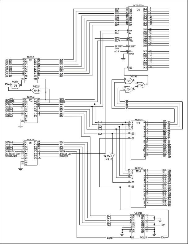
Figure 3.
Schematic diagram
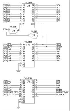
Figure 4. Schematic diagram of buffer section of interface card.
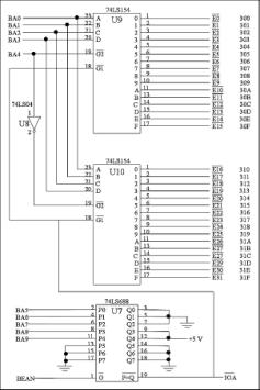
Figure
6. Schematic
diagram of interface section of interface card.
BOARD LAYOUT
The board layout is dependent upon the student, but a logical placement of the ICs on the prototype boards is required. There should be a flow throughout the design to allow ease of wiring and troubleshooting. Figure 8 shows the layout used for the paper.
Figure
8. Board layout
used on the interface card.
INTERFACE
CONNECTOR
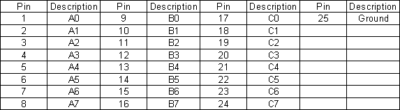
A 25 pin D-sub connector is used to connect the interface card with the outside world. This connector allows for the 24 lines of digital I/O and a ground. The pinout and connector is shown in Figure 9.
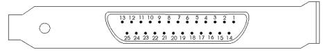
Figure
9. Pinout and
connector of the interface card.
WIRE WRAPPING
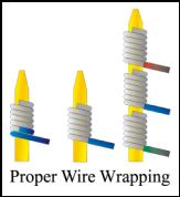
Figure
10. Proper wire
wrapping.
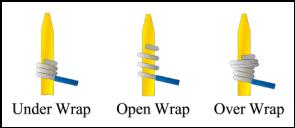
Figure 11.
Improper wire
wrapping examples.
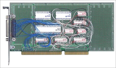
FINISHED BOARD
The top view of the finished interface card is shown in figure 12. The bottom view of the finished interface card is shown in figure 13.
Figure
12. Top view of
interface card.
Figure
13. Bottom view
of interface card.
TESTING INTERFACE CARD
Once the interface card is completed it needs to be tested before being
integrated into a system. A test circuit must be built in order to test the
card. The test circuit is small and consists of LEDs to test the outputs, and
switches to test the inputs. This circuit should be bread boarded because it is
temporary and it is not essential for operation of the card. Although a
permanent test board could be build for future boards and trouble shooting.
Figure 14 is a diagram of the test circuit.
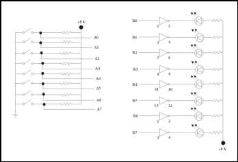
Figure
14. Circuit used
to test the 8255 interface card.
To finish testing the board simple routines need to be programmed in BASIC. These routines will program desired ports as either input or output. The following are programs written to test the interface card. A description of each program is located at the beginning of each program.
|
100 REM READS PORTA AS INPUT AND OUTPUTS TO PORT B 101 REM AS PORT A DIPSWITCH SETTINGS ARE DISPLAYED ON
PORT 102 REM B LEDS 110 BASEADDR = 768: REM 300H 120 PORTA = BASEADDR 125 PORTB = BASEADDR + 1 130 CNTRL = BASEADDR + 3 140 OUT CNTRL, 136 150 D = INP(PORTA) 160 PRINT "PORTA = "; D 170 OUT PORTB, D 180 GOTO 150 |
|
100 REM 8255 PPI Set Ports A,B,C to Output 101 REM USES PORT B AS A PULSE OUT 110 BASEADDR = 768: REM 300H 120 PORTB = BASEADDR + 1 130 CNTRL = BASEADDR + 3 140 OUT CNTRL, 128 145 PRINT "TYPE IN A DELAY LOOP AMOUNT" 146 INPUT D 150 SGNAL1 = 0 155 SGNAL2 = 1 160 OUT PORTB, SGNAL1 170 FOR DELAY = 1 TO D: NEXT DELAY 180 OUT PORTB, SGNAL2 185 FOR DELAY = 1 TO D: NEXT DELAY 190 GOTO 160 |
Figure 15 is a screenshot of a BASIC program used to set all ports as ouput, and set Port B to display a count from 0 to 255 using the LEDs on the test circuit.
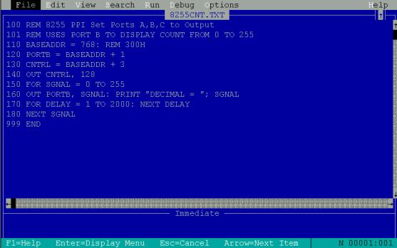
Figure 15. Test program to set Port B to count from 0 to 255.
FUTURE CONSIDERATIONS
Future circuits can be added to the 8255 interface card. The interface card’s decoder circuit is designed to allow future expansion. Other devices such as a timer/counters, ADCs, and DACs can be added to the circuit.
CONCLUSIONS
REFERENCES
Brey,
B. B. (1995). The Intel
32-bit microprocessors: 80386, 80486, and Pentium.
Englewood Cliffs, NJ: Prentice Hall.
Comer,
D. E. (1999). Computer
networks and internets (2nd. Ed.).
Upper Saddle River, NJ: Prentice Hall.
Rafiquzzaman,
M. (1995). Microprocessors and microcomputer-based system
design (2nd Ed).
New York, NY: CRC Press.
Subbaraol,
W. V. (1992). The 8086/
8088 familiy of microprocessors: Software, hardware, and system applications.
Albany, NY: Delmar
Publishers Inc..
Triebel,
W. A. (1998). The 80386,
80486, and the Pentium processor.
Upper Saddle River, NJ: Prentice Hall.
Triebel,
W. A., and Singh, A. (1997).
The 8088 and 8086 microprocessors: Programming, interfacing,
software, hardware, and application (2nd Ed).
Upper Saddle River, NJ: Prentice Hall.
Uffenbeck,
J. (1998). The 80X86
family: Design, programming, and interfacing (2nd Ed.).
Upper Saddle River, NJ: Prentice Hall.