|
|
Volume 3 No.3, Fall 1999 |
ISSN# 1523-9926 |
|
|
Volume 3 No.3, Fall 1999 |
ISSN# 1523-9926 |
Dr. William R. Grisé
w.grise@morehead-st.edu
Department of IET
Morehead State University
ABSTRACT
This paper will explain the basic concepts underlying the operation of the switched capacitor, as well as the use of switched-capacitors to realize compact and versatile circuits already familiar to the undergraduate student of electronics. One set of example circuits include easily tunable active filters; specific examples of filter designs that incorporate switched-capacitors will be developed, and the use of a commercially available switched-capacitor integrated circuit, the MF10, to implement the designs will be shown. Another example circuit is an instrumentation amplifier that is more compact and has a higher CMRR than the conventional realization. Linear Technology's LTC1043 serves as the vehicle for this circuit. By demonstrating the utility of the modern switched-capacitor IC in these two important electronic functions, it is hoped that instructors and students in engineering technology will include the study of the switched-capacitor in advanced electronics courses.
I. INTRODUCTION
This paper aims to show how the
switched-capacitor concept can be used to realize a wide variety of active
filters that have the advantages of compactness and tunability.
In particular, the explanations and design examples presented here will
use mathematical tools familiar to the electronics technology and engineering
undergraduate student. We will not use the Z-transform, which is the rigorously
correct tool for analyzing sampled-data waveforms.
The paper will present the
following topics. First, the basic ideas behind the use of the
switched-capacitor to replace resistors in active filter circuits will be
explained. Second, the use of the
switched-capacitor to implement lossless, lossy, and differential integrators,
which are the backbone of many switched-capacitor filter circuits, especially
those based on National Semiconductor's MF10 IC [1]. Third, example designs of active filters using the MF10 will
be presented.
Before detailing the operation
of switched-capacitor circuits, it will be useful to understand the motivation
behind, and applications of, these circuits. Basically, switched-capacitor
techniques have been developed in order to allow for the integration on a single
silicon chip of both digital and analog functions. Because very large scale
integrated (VLSI) circuits rely on MOS transistors and pico-farad range MOS
capacitors, any realization of analog circuits on a chip will have to use these
elements. By comparison, conventional analog circuits use the ratio
of resistances to set the transfer functions of amplifiers, and the magnitudes
of resistances to determine the operation of current-to-voltage and
voltage-to-current converters. Finally, the values of RC products are
used in active filters and signal generators to determine the frequency
responses of those circuits. When one moves to the silicon chip and strives to
achieve the same functionality in a much reduced area and using the tools of MOS
technology, this is what one discovers. First, switches, small-value capacitors,
and decent op-amps are easy enough to realize in MOS technology. Second, using
that same technology, it is very difficult and wasteful of silicon die area to
make resistors and capacitors with the values and accuracy encountered in audio
and instrumentation applications [2,3]. As we will see in the subsequent
sections, designers have overcome these difficulties by realizing that (1)
resistors can be replaced by MOS switches that are rapidly turned on and off,
and MOS capacitors, and that (2) the time constants arising from these simulated
resistances and the MOS capacitors are given in the form of capacitance ratios.
The fact that capacitor ratios control the time constants means that these
constants now can take advantage of the superior matching of capacitances
fabricated on silicon, as well as their ability to track each other with
temperature.
If these are undoubted
advantages for the VLSI designer, what can the board-level circuit design expect
to achieve with the use of switched-capacitors? For one thing, as we will see
shortly, not only are the time constants of the switched-capacitor circuit
superior in their control, but these time constants are tunable through the
simple expedient of changing the frequency of the clock pulses that drive the
circuit. Furthermore, the integrated circuit packages that are now available
support a number of filtering functions in one package, thus reducing footprints
needed on circuit boards to realize a given set of analog functions.
Although switched-capacitors were developed in order to meet the need to incorporate analog, active filters on silicon along with digital functions, they have since found many other uses [2]. These include, besides filters, instrumentation amplifiers, voltage-to-frequency converters, data converters, programmable capacitor arrays, balanced modulators, peak detectors, and oscillators.
II. BASIC SWITCHED-CAPACITOR OPERATION
The essence of the
switched-capacitor is the use of capacitors and analog switches to perform the
same function as a resistor. This
replacement resistor, along with op-amp based integrators, then forms an active
filter. Before delving too far into
actual filter designs, however, it makes sense to ask why one would want to
replace the resistor with such an apparently complex assembly of parts as
switches and capacitors. It would
seem from the multiplication of parts that the switched-capacitor would be area
intensive. As a matter of fact, for
the resistor values that one seeks in certain filter designs, this is not the
case. Furthermore, the use of the
switched-capacitor will be seen to give frequency tunability to active filters.
Figure 1[2, 3] shows the basic setup for a switched-capacitor, including
two N-channel Metal-Oxide Semiconductor Field-Effect
Transistors (NMOS) and a capacitor.
There are two clock phases,
![]() , which are non-overlapping. The MOSFET's, either M1 or M2, will be turned ON
when the gate voltage is high, and the equivalent resistance of the channel in
that case will be low,
, which are non-overlapping. The MOSFET's, either M1 or M2, will be turned ON
when the gate voltage is high, and the equivalent resistance of the channel in
that case will be low,
![]() . Conversely, when the gate voltage goes LOW, the channel resistance will look
like
. Conversely, when the gate voltage goes LOW, the channel resistance will look
like
![]() . With such a high ratio of OFF to
ON resistances, each MOSFET can be taken for a switch. Furthermore, when the two
MOSFET's are driven by non-overlapping clock signals, then M1 and M2 will
conduct during alternate half-cycles.
. With such a high ratio of OFF to
ON resistances, each MOSFET can be taken for a switch. Furthermore, when the two
MOSFET's are driven by non-overlapping clock signals, then M1 and M2 will
conduct during alternate half-cycles.
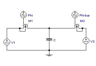
Figure 1. Two NMOSFET's,
driven by alternating, non-overlapping clock signals, comprise the basic
switched capacitor network.
This makes the two-MOSFET
arrangement equivalent to a single-pole, double-throw switch (SPDT).
One can now use a symbolic switch picture, as in Figure 2a below, to
represent the circuit. The operation of this circuit is as follows. When the switch
is thrown to the left, the capacitor will charge up to
![]() . When the switch is thrown to the right, the capacitor will discharge down
to/charge up to
. When the switch is thrown to the right, the capacitor will discharge down
to/charge up to
![]() . As a result of these consecutive switching events, there will be a net charge
transfer of
. As a result of these consecutive switching events, there will be a net charge
transfer of
![]() . Now, if one flips the switch back
and forth at a rate of
. Now, if one flips the switch back
and forth at a rate of
![]() cycles/sec, then the charge
transferred in one second is
cycles/sec, then the charge
transferred in one second is
![]() , which of course has the units of current.
One can claim that an average current,
, which of course has the units of current.
One can claim that an average current,
![]() . If
. If
![]() is much higher than the frequency
of the voltage waveforms, then the switching process can be taken to be
essentially continuous, and the switched-capacitor can then be modeled as an
equivalent resistance, as shown below in Figure 2b.
The value of the equivalent resistance is given by:
is much higher than the frequency
of the voltage waveforms, then the switching process can be taken to be
essentially continuous, and the switched-capacitor can then be modeled as an
equivalent resistance, as shown below in Figure 2b.
The value of the equivalent resistance is given by:
![]() (Eq. 1)
(Eq. 1)
Therefore, this equivalent resistance, in conjunction with other capacitors, and Op-amp integrators, can be used to synthesize active filters. It is now clear from Equation (1) how the use of the switched-capacitor leads to tunability in the active filters, by varying the clock frequency.
(a) (b)
Figure 2. Equivalent resistor model for switched capacitor circuit
in Fig. 1.
This equivalent resistance has
features which make it advantageous when realized in integrated-circuit form:
(a) High-value resistors can be implemented in very little silicon area. For example, a 1-MW resistor can be realized with a 10-pF capacitor switched at a clock rate of 100 kHz.
(b) Very accurate time constants can be realized, because the time constant is proportional to the ratio of capacitances, and inversely proportional to the clock frequency:
![]() . Capacitor ratios, especially in monolithic form, are very robust against
changes in temperature, and clock frequencies can also be strictly controlled,
so that accurate time constants are now available in the switched-capacitor
technology.
. Capacitor ratios, especially in monolithic form, are very robust against
changes in temperature, and clock frequencies can also be strictly controlled,
so that accurate time constants are now available in the switched-capacitor
technology.
The principal constraint in
using the switched-capacitor is that inherent in all sampled-data systems: the
clock frequency must be much higher than the critical frequency set by the RC
products in the circuit. Furthermore, on either side of the analog switches,
i.e., the MOSFET's, there must be essentially zero-impedance nodes (voltage
sources). There are a number of
other constraints which the unsuspecting designer/user might overlook [3, p.
725]:
(a) The equivalent resistance formed by the action of the switched-capacitor cannot be used to close the negative-feedback path in an op-amp all by itself. One must recall that to ensure stability, the op-amp's feedback path must be closed continuously, while the switched-capacitor is a sampled-data construction of a resistor, and thus not continuous.
(b) Circuit nodes cannot be left floating. That is, there must always be a resistive path to ground so that charge does not build up on the capacitor plates.
(c) The bottom plates of the MOS capacitors must be connected to ground or to a voltage source. There is an intrinsic, parasitic capacitance associated with the MOS capacitor's bottom plate [4]. This parasitic capacitance can be between 5% and 20% of the desired value; furthermore, it behaves nonlinearly with voltage [4]. Therefore, it must be connected to AC ground or a voltage source so that this nonlinear portion of the capacitance will not affect the overall response of the switched-capacitor filter. In practical terms, this means that capacitive voltage dividers with three or more capacitors, and circuits that switch both ends of a capacitor in sequence to the inputs of an op-amp, are used.
(d)
The noninverting pin of the op-amp should be kept at a constant voltage.
If this pin is connected to the signal in some way, then the virtual short
circuit between op-amp inputs means that the inverting input is no longer a
virtual ground, and so an undesirable alteration of filter response due to the
MOS capacitor's parasitic capacitance will occur (see item (c) above).
III. SWITCHED CAPACITOR INTEGRATORS
The op-amp integrator is the
most frequently chosen building block for switched-capacitor filters.
The standard RC integrator is shown in Figure 3a, and its analysis and
description can be found in any electronics text [5, 6].
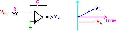
Figure 3a. Standard op-amp integrator, with transfer curve
To review, the voltage transfer function of this circuit is given by
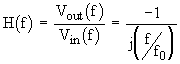 (Eq. 2)
where
![]() . Now, if one replaces the resistor by its switched-capacitor equivalent, as
shown in Figure 3b, and use Eq. 1 as the resistor's value, one finds
. Now, if one replaces the resistor by its switched-capacitor equivalent, as
shown in Figure 3b, and use Eq. 1 as the resistor's value, one finds
![]() (Eq. 3)
(Eq. 3)
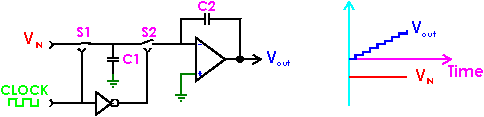
Figure 3b. Switched-capacitor integrator.
![]() , depends on a ratio of capacitances, not on an RC product.
The tolerances for ratios are much easier to control than the tolerances
for products. Finally, this characteristic frequency of the integrator is
inherently settable with a simple change in the clock frequency.
, depends on a ratio of capacitances, not on an RC product.
The tolerances for ratios are much easier to control than the tolerances
for products. Finally, this characteristic frequency of the integrator is
inherently settable with a simple change in the clock frequency.
The typical values of
capacitances used in switched-capacitor technology range from 0.1 pF to 100 pF.
These are low enough values that the stray capacitances of the MOS switches, of
the interconnects, and of the "plates" of the switched-capacitors
themselves can all have a significant effect on the desired frequency response
of the filters designed with switched-capacitors. The effects of stray
capacitance have been reduced greatly by dual-switch configurations [2, 7].
Figure 4 shows explicitly the clock phasing of the MOS switches which acts to
eliminate the transient charge transfer through the stray capacitances, Cs1 and
Cs2, also indicated in the figure. In
essence, charge transfer only takes place through the capacitor
![]() . Figures 5a and 5b show both the inverting and noninverting stray-insensitive
integrator. The noninverting stray-insensitive integrator is obtained simply by
switching the clock phasing on transistors M2 and M4.
. Figures 5a and 5b show both the inverting and noninverting stray-insensitive
integrator. The noninverting stray-insensitive integrator is obtained simply by
switching the clock phasing on transistors M2 and M4.
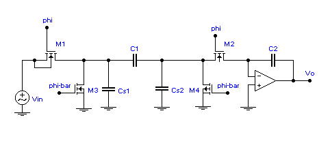
Figure 4. Arrangement of extra MOSFET's and clock signals to make switched capacitor circuit insensitive to stray capacitances.
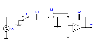
Figure 5a. Switch setting used to realize stray-insensitive inverting integrator.
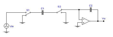
Figure 5b. Switch setting for stray-insensitive non-inverting integrator.
Because of the importance of the
integrator to switched-capacitor filters, it is necessary to be familiar with
the variants of the integrator. These
include the summing integrator, the differential integrator, the
integrator/summer, and the lossy integrator. All of these play a role in the
synthesis of switched-capacitor filters. The summing integrator, shown below in
Figure 6, has a response given by:
 (Eq. 4)
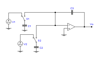
Figure 6. Summing integrator.
Figure 7 shows the differential
integrator. The easiest way to
understand this circuit is to look at what happens to the charge accumulation on
the capacitor
![]() when the switches are thrown to the
left. In this case, the capacitor
charges up to a value of
when the switches are thrown to the
left. In this case, the capacitor
charges up to a value of
![]() . When the switches are thrown to the right, the charge on the capacitor is
poured into the op-amp's summing node. The average current, assuming the
switching rate (= clock frequency) is high enough, is given by
. When the switches are thrown to the right, the charge on the capacitor is
poured into the op-amp's summing node. The average current, assuming the
switching rate (= clock frequency) is high enough, is given by
![]()
![]() (Eq. 5)
(Eq. 5)
This results in a
stray-insensitive output voltage of
 (Eq. 6)
where
![]() .
.
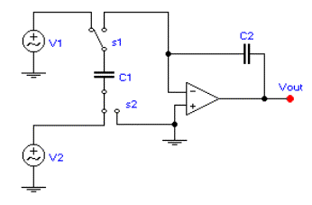
Figure 7. Differential integrator.
The lossy integrator
provides a simple, first-order lowpass response with gain. This circuit is
realized by placing a switched-capacitor (i.e., a simulated resistor) in
parallel with a feedback capacitor, Figure 8. In general, the easiest way to
analyze the response of more complex switched-capacitor circuits such as this
one is to replace all switched-capacitors with their resistor equivalents. Once
the transfer function is found for a circuit with resistors (and discrete
capacitors), then the switched-capacitor equivalents of the resistors (Eq. 1)
can be placed back in the transfer function to obtain the final result. For the
lossy integrator, the analysis proceeds as follows:
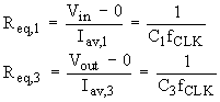
where the "0" in
![]() refers to the virtual ground at the
op-amp's inverting input. The transfer function is obtained using these resistor
equivalents:
refers to the virtual ground at the
op-amp's inverting input. The transfer function is obtained using these resistor
equivalents:
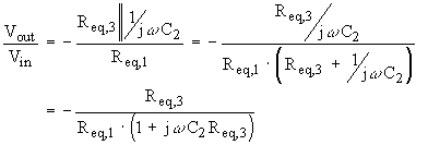 (Eq. 7)
Now substituting the switched-capacitor equivalents for the resistors from Eq. 1, one obtains
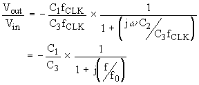 (Eq. 8)
where
![]() is the critical, or -3 dB,
frequency of the lowpass filter. Eq.
8 has the form of a lowpass filter multiplied by a gain proportional to the
ratio of the two switched-capacitors.
is the critical, or -3 dB,
frequency of the lowpass filter. Eq.
8 has the form of a lowpass filter multiplied by a gain proportional to the
ratio of the two switched-capacitors.
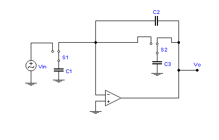
Figure 8. Lossy integrator, or first-order lowpass filter with gain.
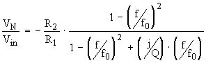
IV. SWITCHED CAPACITOR BIQUADRATIC FILTERS
The biquad configuration [8] normally features a lossy
inverting integrator, a lossless inverting integrator, and a
unity-gain-inverting amplifier. In the standard active RC configuration, this requires three
op-amps. However, the
switched-capacitor realization of the biquad needs only two op-amps to perform
the same function. One op-amp performs the lossy inverting integration function,
while the second op-amp performs lossless, noninverting integration. Although
one can design an adequate switched-capacitor version of the biquad by making a
resistor-by-resistor replacement in the standard RC biquad filter, such an
implementation has been found to have unacceptably wide capacitance spreads,
especially when higher filter Q's are sought [2]. Instead, Figure 9 shows the
biquad filter with improved capacitance ratios. This circuit provides the
highpass and bandpass responses. Just as with the analysis of the lossy
integrator, a fairly complete analysis of this circuit will be made here.
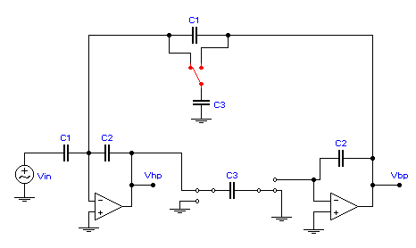
Figure 9. Biquadratic
bandpass and highpass filter provided by switched capacitor network, with
improvements needed to reduce spread in capacitor values.
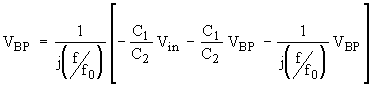
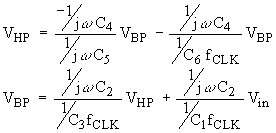
The form of the bandpass
filter function is at least clear:
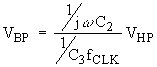 (Eq. 9)
The use of a stray-insensitive
switched-capacitor (
![]() ) with alternating clock phases makes possible the noninverting form above. In
order to complete the analysis, one has to calculate the highpass filter
response. The output node of the
first op-amp, which gives the highpass filter response, can be seen to be the
superposition of two signals at the summing node of the op-amp:
) with alternating clock phases makes possible the noninverting form above. In
order to complete the analysis, one has to calculate the highpass filter
response. The output node of the
first op-amp, which gives the highpass filter response, can be seen to be the
superposition of two signals at the summing node of the op-amp:
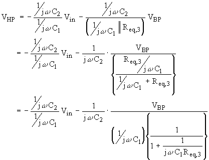 (Eq. 10a)
With
![]() the expression in curly brackets
simplifies, giving
the expression in curly brackets
simplifies, giving
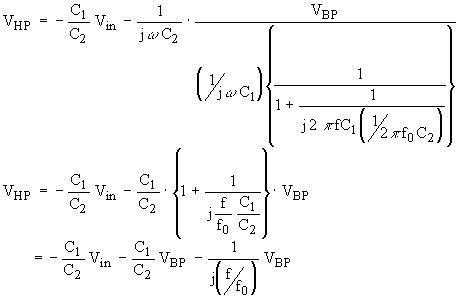 (Eq. 10b)
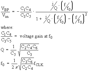
In order to obtain finally
the bandpass transfer function, Eq. 10b is inserted into Eq. 9. The result of
this manipulation is
![]()
 (Eq. 11)
Gathering like terms together,
and multiplying both sides by
![]() , one obtains
, one obtains
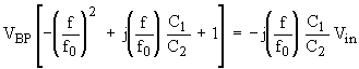 (Eq. 12)
With
![]() , and isolating
, and isolating
![]() , the transfer function for the bandpass filter is finally found:
, the transfer function for the bandpass filter is finally found:
 (Eq. 13)
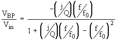
The corresponding
expression for the highpass filter is simply obtained by inverting Eq. 9.
Recalling that
![]() , one finds readily
, one finds readily
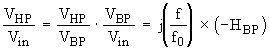 (Eq. 14)
Although Eq. 13 does in
fact display the standard form for the frequency
response of a bandpass filter, there is nothing in the expression that gives the
gain of the filter circuit. In
fact, from the form of the transfer function, and from simulation, it can be
seen that the circuit in Figure 9 has no resonant gain. The same applies to the
highpass filter expression in Eq. 14. It
is clear that a useful active filter circuit formed from switched-capacitors
must possess some voltage gain in the passband. Of course, it is possible to
simply "tack on" an amplifier to the output of the circuit. However,
an elegant solution is to turn the second op-amp in Figure 9 into a summing
integrator, in which the input signal is injected into the second op-amp via an
equivalent resistance derived from another switched-capacitor. Figure 10 shows
the implementation of this idea. In Figure 10, the SPDT switches, labeled S1,
are shown closed in the first half of the clock cycle
![]() .
.
The analysis of this circuit in
order to derive the bandpass filter transfer function follows a path similar to
the one followed in Eq. 13, although more tedious. We will simply present the
main results here and proceed to the simulation of the circuit.
Superposition of input signals to each of the op-amp's input pins gives
 (Eq. 15)
After much manipulation,
one finds that the transfer function for the bandpass filter is
 (Eq.
16)
(Eq.
16)
In order to simulate the
performance of switched-capacitor networks, it is necessary to realize that
these circuits are a hybrid of both continuous and sampled-data signals.
In fact, switched-capacitor circuits are continuous in amplitude and
discrete in time. Because of this combination, simulation with conventional
circuit simulators such as PSPICEÔ
presents a problem. The presence of switched voltages means that a transient
analysis must be performed. At the same time, the desire to determine the
frequency response across a wide range of frequencies means that a transient
analysis must be performed for each desired frequency. This is a very
time-consuming process because one has to wait until the steady state is
reached. One way to overcome this problem within a SPICE-type simulator is to
implement all the design equations in z-transforms. These z-domain models will
allow one to perform frequency-domain simulation of complex switched-capacitor
circuits. Although the z-transform is the rigorously correct mathematical tool
for the analysis of sampled-data systems, it is not really available to the
majority of engineering technology students. The model element used as the
simulation kernel in SPICE for z-domain analysis is called the storistor
[10]. It consists of conductances, a lossless transmission line for delay
effects, and controlled sources. In order to simulate the frequency response of
something as simple as an integrator, one is required to model as many as seven
storistors, four capacitors, and an op-amp subcircuit. Given the long experience
of many students and instructors with the SPICE program, this might be an
acceptable alternative. However, the size of the input files for even simple
switched-capacitor circuits (beyond the integrator), together with the
mathematics required to understand the z-transform, will probably deter many
from this approach.
This paper will use a perhaps
less well-known simulation package called APLACÔ
[11-12] (originally Analysis Program for Linear Active
Circuits). The APLAC program has been under continuous development
since 1972. Since 1988, the Nokia Corporation, developers of wireless
communication products, has sponsored continued improvement in the system design
and electromagnetic capabilities of the APLAC program. The particular strengths
of the APLAC program are its use of object oriented programming techniques,
which permit easy adaptation of models to the circuit environment in which a
component finds itself. Also, the program has a very extensive library of system
level blocks, and the ability to model electromagnetic behavior of components.
For our present purposes, one of
the attractions of the APLAC program is its use of the convolution integral to
model circuits with both frequency-dependent and transient behaviors. This
feature is important for switched-capacitor circuits. The frequency-dependent
portions of the circuit can be analyzed straightforwardly. However, the
frequency response of the time-dependent portions of the circuit (such as
switches and sources) is calculated by creating a frequency-domain equivalent
circuit by means of the convolution integral.
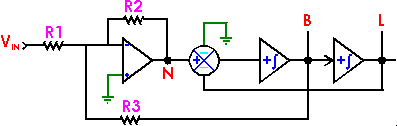
In the circuit of Figure 10, the
following values of components and parameters are used:
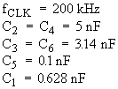
These values give a resonant (center frequency) voltage gain of A0 = 10, a Q = 50, and a center frequency of f0 = 20 kHz. The results of the simulation are shown below, in Figure 11.
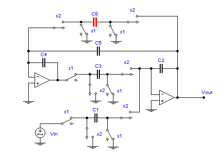
Figure 10. Biquadratic switched-capacitor filter with gain setting
from summing integrator. The switches S1 are closed on the first half-cycle of
the clock waveform.
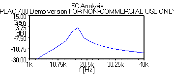
Figure 11. APLAC simulation of bandpass filter with gain, from Figure 10. From Probe tool of simulator, peak gain is 3.32 dB, and center frequency is at f0 = 17.8 kHz.
The results show a simulated gain of only 3.3 dB, and the center frequency is off by ~2 kHz. This inaccuracy is due to the use of ideal MOS switches in the hand calculations leading up to Eq. 16. The APLAC model for the switches assumes an Ron = 100 W, and an Roff = 100 kW. APLAC has the capability to optimize the circuit's component values to achieve desired circuit behaviors.
V. APPLICATION OF MF-10
The MF-10 is a universal
switched-capacitor filter supplied by National Semiconductor [1]. The MF-10 uses
the two-integrator loop structure to realize lowpass, highpass, bandpass, notch,
and allpass functions through externally chosen, discrete, resistors. The actual
switched-capacitor integrators are internal to the chip, while the external
resistors give the user flexibility in configuring his/her own response.
However, to take advantage of component tracking with temperature, etc., all
responses are designed to be functions of resistor ratios only.
Figure 12 shows the summing amplifier and two-integrator cascade internal
to each section of an MF-10. The tunability of a particular filter's critical
frequency,
![]() , is determined by a logic level applied to a 50/100/CL frequency ratio
programming pin. In other words, the critical frequency will be
, is determined by a logic level applied to a 50/100/CL frequency ratio
programming pin. In other words, the critical frequency will be
![]() ; if the programming pin is tied to ground, the divisor is 100, otherwise, if
tied to a HIGH (positive power supply), the divisor will be 50. Figure 12 shows
how the notch, bandpass, and lowpass filter functions are realized by the MF-10.
Because the summing amplifier is outside the two-integrator loop, this
configuration will be faster and allow a greater range of operating frequencies.
; if the programming pin is tied to ground, the divisor is 100, otherwise, if
tied to a HIGH (positive power supply), the divisor will be 50. Figure 12 shows
how the notch, bandpass, and lowpass filter functions are realized by the MF-10.
Because the summing amplifier is outside the two-integrator loop, this
configuration will be faster and allow a greater range of operating frequencies.
Figure
12. Two-integrator loop, with external resistors, used in MF-10 to realize
notch, lowpass, and bandpass filters.
The analysis of the transfer
functions for the three transfer functions mentioned above follows the pattern
in Eq. 13-14. By inspection, one sees that
 (Eq. 17a)
 (Eq. 17b)
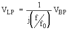 (Eq. 17c)
Eliminating
![]() to obtain
to obtain
![]() , the transfer function for the notch filter is obtained:
, the transfer function for the notch filter is obtained:
 (Eq. 18)
Similar manipulations give the bandpass and lowpass responses. The bandpass response is:
 (Eq. 19)
The lowpass response is:
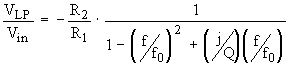 (Eq. 20)
Although
the initial impetus for the development of the switched-capacitor was the
opportunity and need to synthesize active filters that would be compatible with
MOSFET technology, the early 1980's found many other uses for the
switched-capacitor. Linear Technology has developed the LTC1043 [9], which
contains dual switched capacitor networks, along with an on-chip non-overlapping
clock generator, oscillator, and charge balancing circuitry. The clock generator
controls both of the switch networks, while the charge balancing circuitry is
designed to cancel any effects due to stray capacitance. The on-chip oscillator
has a fixed frequency of 185 kHz. An external capacitor can be connected across
pins 16 and 17 (for the instrumentation amplifier) to yield any desired clock
rate. The desired clock rate can be found from
![]() ; the 24-picofarad capacitance is the internal capacitance responsible for the
oscillator’s fixed frequency.
; the 24-picofarad capacitance is the internal capacitance responsible for the
oscillator’s fixed frequency.
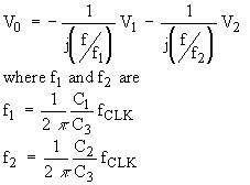
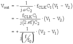
Among the circuits developed from the LTC1043 are instrumentation amplifiers, lock-in amplifiers for detecting extremely small parameter shifts in sensor applications, and signal conditioners for platinum resistance temperature detectors (RTD), relative humidity sensors, and LVDT’s. The instrumentation amplifier is a standard op-amp circuit presented in many electronics texts [5-6], and is designed to amplify small difference signals such as might be found in measurement or transducer applications. At the same time, common-mode or noise signals picked up by the lines feeding the amplifier must be suppressed, especially as these signal levels are often larger in amplitude than the sought-for difference signals. Figure 13 shows the LTC1043 combined with a standard non-inverting op-amp to give an instrumentation amplifier with a common-mode rejection ratio (CMRR) of >120 dB. Figure 14 shows the same circuit with the ½ LTC1043 as a black box.
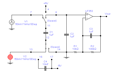
Figure 13. Instrumentation amplifier using ½ of LTC 1043
switched-capacitor, along with LF356/353 op-amp in non-inverting configuration.
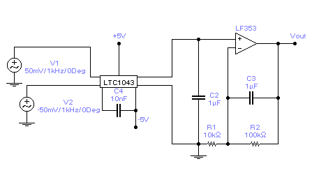
Figure 14. Switched-capacitor-based instrumentation amplifier, with
½ LTC1043 shown as a black box. The pin numbers in Figure 13 are the pins in
the black box in this figure.
The
operation of this circuit is as follows. First, the dual switch, when flipped to
the left, charges the capacitor C1 up to the difference V1
– V2. Second, on the next clock pulse, the switches will then dump
the charge represented by that voltage difference onto C2. Third, the
continuous clocking from the oscillator will force C2 to eventually
develop a voltage equal to the difference voltage. Finally, the difference
voltage, with the common-mode signal stripped off by the LTC1043 is amplified by
the op-amp. It is interesting to observe several features of this circuit and
compare them to the standard instrumentation amplifier. By using the capacitor C1
(the so-called “flying capacitor”), the common-mode voltage present at the
inputs is looking into a capacitive voltage divider, between the C1
and the LTC1043’s parasitic capacitance. This parasitic capacitance is
typically less than 1 picofarad, so the AC value of the CMRR is > 120 dB. By
comparison, Analog Device’s AD624 instrumentation amplifier can go as high as
130 dB for high gains, up to 60 Hz. Because of the capacitive voltage divider
from the LTC1043, this instrumentation amplifier shows higher CMRR, over a wider
range of voltage gains, and to a higher frequency.
VII.
CONCLUSIONS
This paper has presented the
essentials of operation of
switched-capacitor networks, with a special emphasis on its use in designing
active filters. Unlike active filters based on the conventional op-amp,
switched-capacitor filters have critical frequencies that are easily
pin-settable. Furthermore, they require less power than the conventional op-amp
based network because of their reliance on CMOS technology. Finally, for the
functionality provided on a single chip, they take up less room on circuit
boards. Alternate use of the switched-capacitor network in an instrumentation
amplifier has also been presented. The operation of this device is a little
easier to digest for some students than discussion of active filters; it is
hoped that instructors and students can use the information herein to extend
their acquaintance with modern integrated circuits.
The presentation of results here is in a form which instructors and upper-level students in electronics technology can adapt to the curriculum in technology programs.
REFERENCES
1.
Introducing the MF-10: A Versatile
Monolithic Active Filter Building Block, by Tim Regan. National
Semiconductor Application Note 307, August 1982.
2.
Design with Operational Amplifiers
and Analog Integrated Circuits, by Sergio Franco. McGraw-Hill Book
Company, New York, 1988. Chap. 13.
3.
Bipolar and MOS Analog Integrated
Circuit Design, by A.B. Grebene. Wiley-Interscience, John Wiley &
Sons, New York, 1984. Chap. 13, pp. 703-752.
4.
Fundamentals of MOS Digital
Integrated Circuits, by J.P. Uyemura. Addison-Wesley, Reading, MA, 1988.
Chap. 8.
5.
Electronic Devices, 5th
Edition, by T. L. Floyd. Prentice-Hall, Englewood Cliffs, NJ, 1997.
Chap. 14.
6.
Microelectronic circuits, 3rd
Edition, by A. Sedra and K.C. Smith. Saunders College Publishing/HRW,
Philadelphia, PA, 1991. Chap. 2.
7.
"Stray Capacitance Insensitive Switched Capacitor Filters," M.
Hasler. Proceedings of the IEEE International Symposium on Circuits and Systems,
1981.
8.
Analog Filter Design, by
M.E. Van Valkenburg. Holt,
Rinehart, and Winston, New York, 1982. Chap.
5.
9.
Applications for a
Switched-Capacitor Instrumentation Building Block, by Jim Williams.
Linear Technology Application Note 3, July 1985.
10.
CMOS Analog Circuit Design, 2nd
Edition, by P. Allen and D. Holberg. Saunders College Publishing/HRW,
Philadelphia, PA, 1998. Chap. 9.
11.
APLACÔ
7.0 User's Manual, Helsinki University of Technology, Circuit Theory
Laboratory & Nokia Corporation Research Center, 1998. Available at http://www.aplac.hut.fi/
12.
"Fast Analysis of Nonideal Switched-Capacitor Circuits using
Convolution," H. Jokinen, M. Valtonen, and T. Veijola. 11th
European Conference on Circuit Theory and Design, Davos, Switzerland, 1993,
pp.941-946.